

Charged particle beam apparatus and pattern measuring method
a technology of chargeable particles and beams, applied in the direction of material analysis using wave/particle radiation, instruments, nuclear engineering, etc., can solve the problems of large residual error (difference between actual measured value and expected value), increase in the amplitude of retarding voltage at each measuring point, etc., and achieve the effect of quick processing of many measurement points on the substra
- Summary
- Abstract
- Description
- Claims
- Application Information
AI Technical Summary
Benefits of technology
Problems solved by technology
Method used
Image

Examples
first embodiment
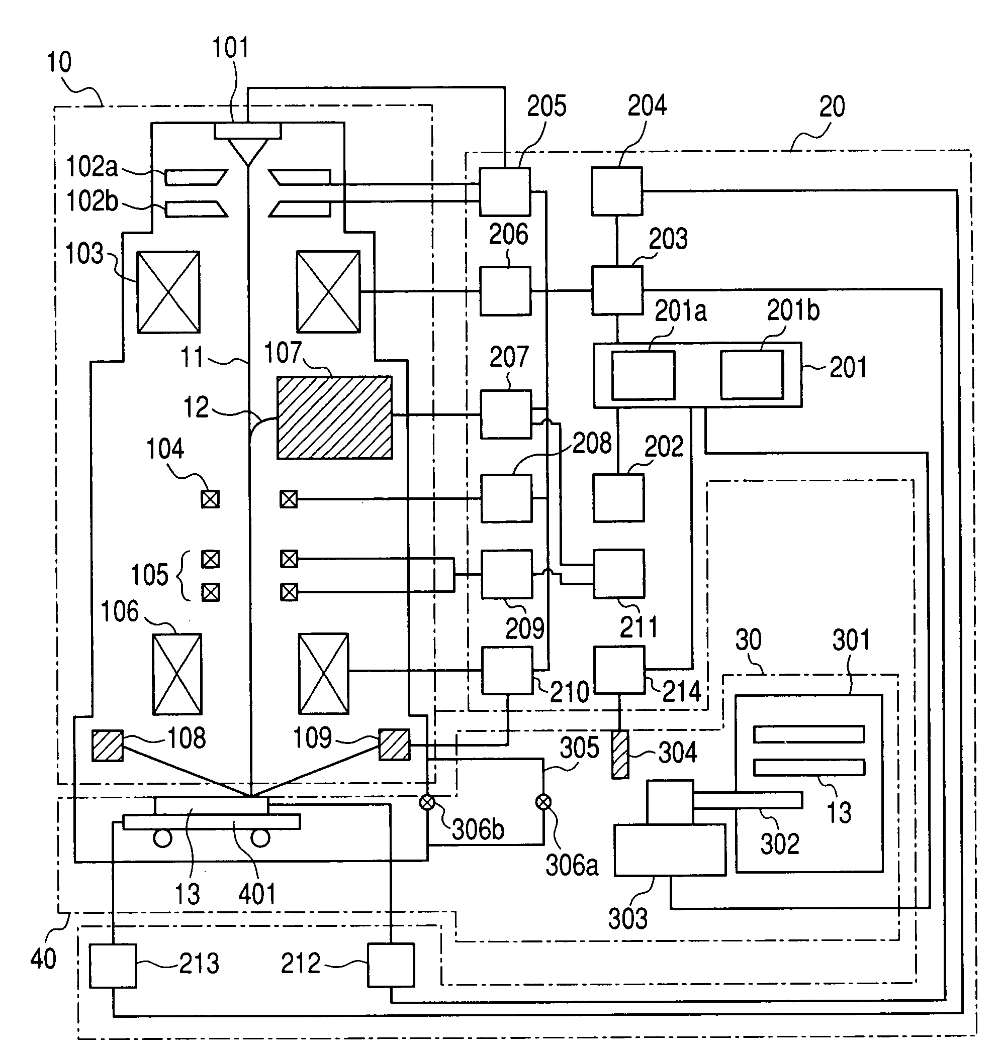
[0031]FIG. 1 is a schematic block diagram of a scanning electron microscopy apparatus to which a first embodiment of the invention is applied.
[0032]As shown in the figure, the scanning electron microscopy apparatus of the embodiment includes charged particle optics 10, a control system 20, a substrate carrier 30, and a substrate chamber 40.
[0033]The charged particle optics 10 includes: a charged particle source 101 for outputting a primary charged particle beam 11; extracting electrodes 102a, 102b; a condenser lens 103; an alignment coil 104; a deflection coil 105; an objective lens 106; a secondary charged particle detector 107 for detecting a secondary charged particle 12; a laser source 108; and a position sensor 109.
[0034]The control system 20 includes: a control system 201; a user interface 202; an optics control system 203; a stage control system 204; an acceleration control system 205; a condenser lens control system 206; an amplifier 207; an alignment control system 208; a d...
second embodiment
[0081]In the above described first embodiment, the surface potential distribution function of the wafer 13 is generated by the best fit model function to the measured data among the plurality of predetermined model functions. On the other hand, in this embodiment, the surface potential distribution function of the wafer 13 is generated by interpolating the surface potential between measured data. Further in the above described first embodiment, the variance σf at a measurement point was used to determine the amplitude Vvar of the retarding voltage Vr at this measurement point. On the other hand, in this embodiment, the surface potential that the surface potential distribution function can take in a predetermined area including a measurement point is used to determine the amplitude Vvar of the retarding voltage Vr at this measurement point. The general configuration of the scanning electron microscopy apparatus to which the present embodiment is applied is the same in the first embod...
third embodiment
[0098]As a third embodiment of the invention, a description will be given taking as an example the case where patterns on the wafers 13 produced in the same lot or process are measured by the scanning electron microscopy apparatus of the first embodiment in mass production line.
[0099]FIG. 8 is a flowchart illustrating the operation procedure for measuring patterns on the wafers 13 produced in the same lot or process by the scanning electron microscopy apparatus of the first embodiment of the invention.
[0100]First the control system 201 uses the charged plate monitor 214 to measure the surface potential of the target wafer 13 (S201). As described above, the charged plate monitor 214 is taken out from the wafer cassette 301 by the probe 304, measures the surface potential at a plurality of points on the line (diameter) including the center of the wafer 13 carried into the substrate exchange chamber 305, and sends the measurement results to the control system 201. The control system 20...
PUM
 Abstract
Description
Claims
Application Information