
Amplifier circuit and wireless communication device

a wireless communication device and amplifier technology, applied in amplifiers, amplifiers with semiconductor devices/discharge tubes, amplifiers, etc., can solve the problems of low gain distortion characteristic, low gain gain gain gain drop, and inability to solve simultaneously, so as to prevent gain loss and improve distortion characteristic

Inactive Publication Date: 2010-02-23
COLLABO INNOVATIONS INC
View PDF4 Cites 1 Cited by
  • Summary
  • Abstract
  • Description
  • Claims
  • Application Information

AI Technical Summary

Benefits of technology

"The present invention aims to enable an amplifier circuit that can prevent loss of gain in the high gain mode, improve distortion in the low gain mode, and set the desired gain. This is achieved by parallel connecting the main load impedance and an impedance circuit that attenuates the gain, so that the load in the low gain mode is the impedance of the parallel connection and the load in the high gain mode is electrically isolated from the parallel connected impedance circuit and is the impedance of the main load impedance. This amplifier circuit can increase gain without increasing current consumption in the high gain mode and reduce distortion and noise in the low gain mode. It can also minimize variation in input / output impedance when switching between the high gain mode and low gain mode."

Problems solved by technology

A first problem with the prior art described above is that gain drops in the high gain mode.
A second problem with the prior art is that is a drop in the distortion characteristic of the low gain mode apparent at the third order input intercept point (IIP3) or the 1-dB compression point (P1 dB).
This also conflicts with the solution to the first problem.
Solutions to the foregoing first and second problems are thus a trade-off, and cannot be simultaneously solved.

Method used


Image

  • Amplifier circuit and wireless communication device
  • Amplifier circuit and wireless communication device
  • Amplifier circuit and wireless communication device

Examples


embodiment 1

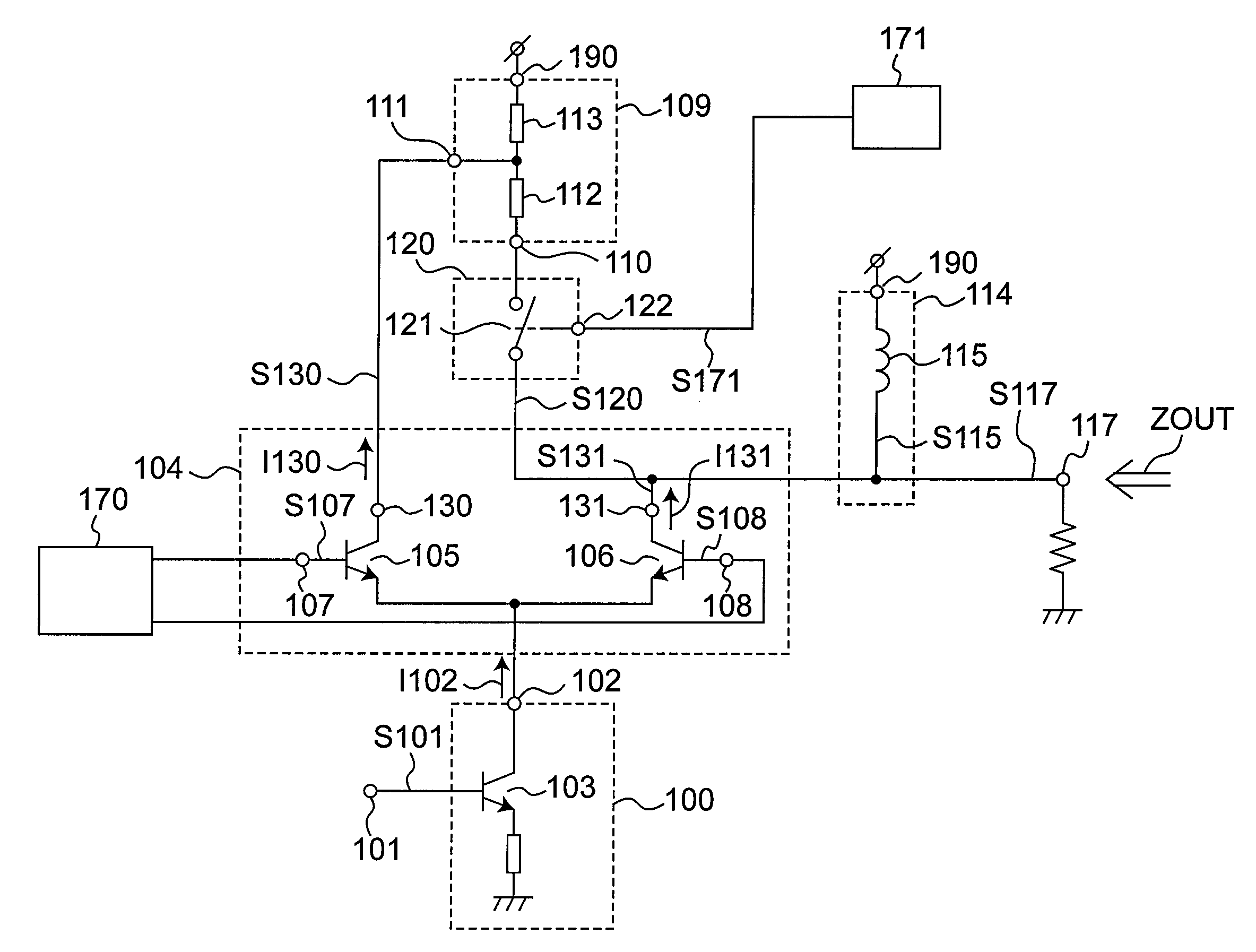
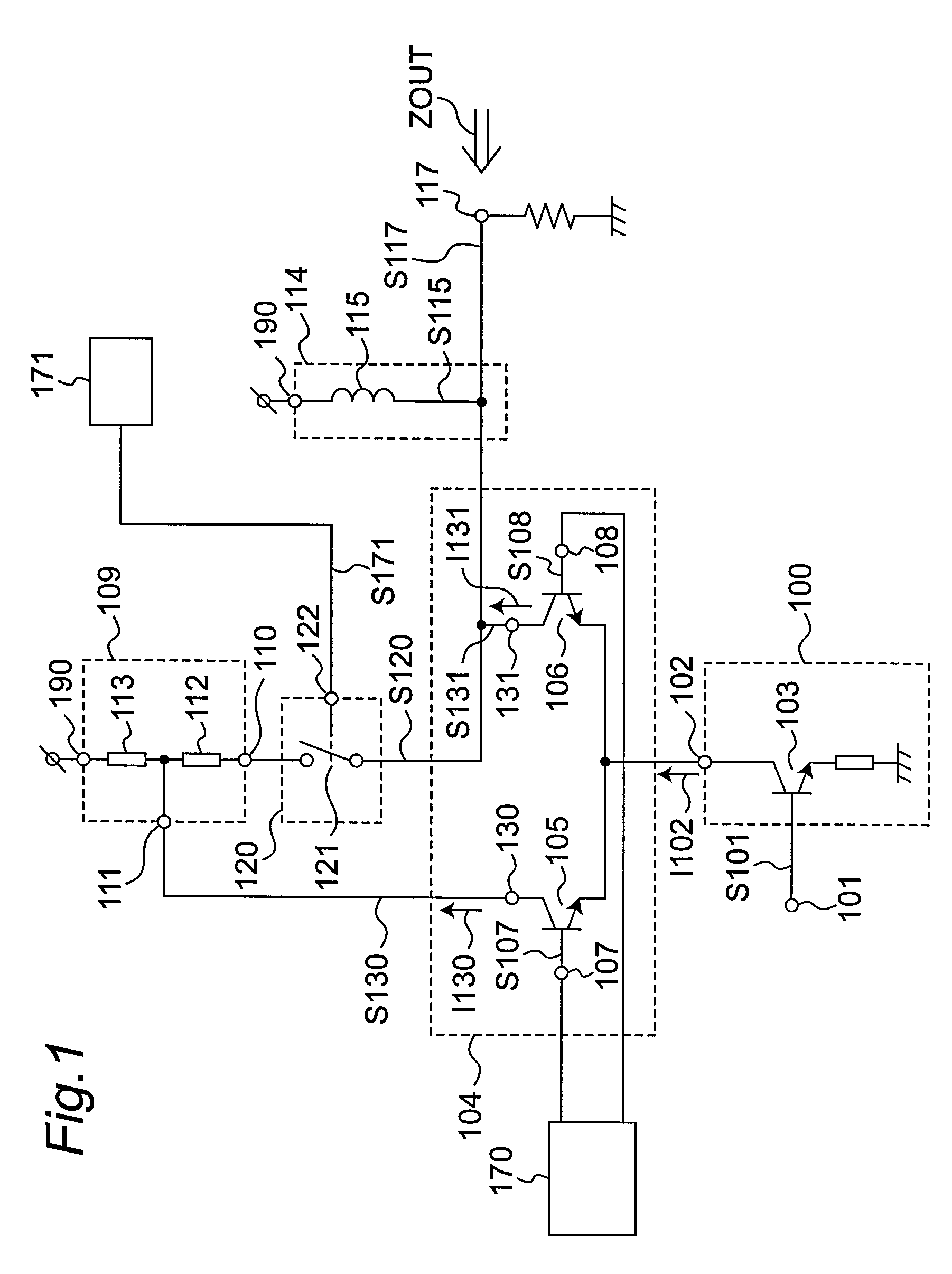
[0058]FIG. 1 is a circuit diagram of an amplifier circuit according to a first embodiment of the invention. As shown in FIG. 1 a high frequency signal S101 to be amplified is input to a current conversion circuit 100 through an input pin 101. The high frequency signal S101 is received at the base of a grounded-emitter transistor 103, and a signal current I102 corresponding to the high frequency signal S101 is then output through the collector of the transistor 103 from the output node 102 of the current conversion circuit 100.

[0059]The signal current I102 is then input to a gain control circuit 104 connected in common to the output node 102. The gain control circuit 104 consists of transistors 105 and 106 having the emitters connected in common. The gain control circuit 104 selectively outputs the signal current I102 to the collectors 130, 131 of the transistors 105 and 106, respectively, based on the control signals S107, S108 from a control signal generating circuit 170 applied to...

embodiment 2

[0071]A second embodiment of the invention is described next focusing on the differences with the first embodiment. Other aspects of the arrangement, operation, and effect of the second embodiment are the same as in the first embodiment, and further description thereof is omitted below.

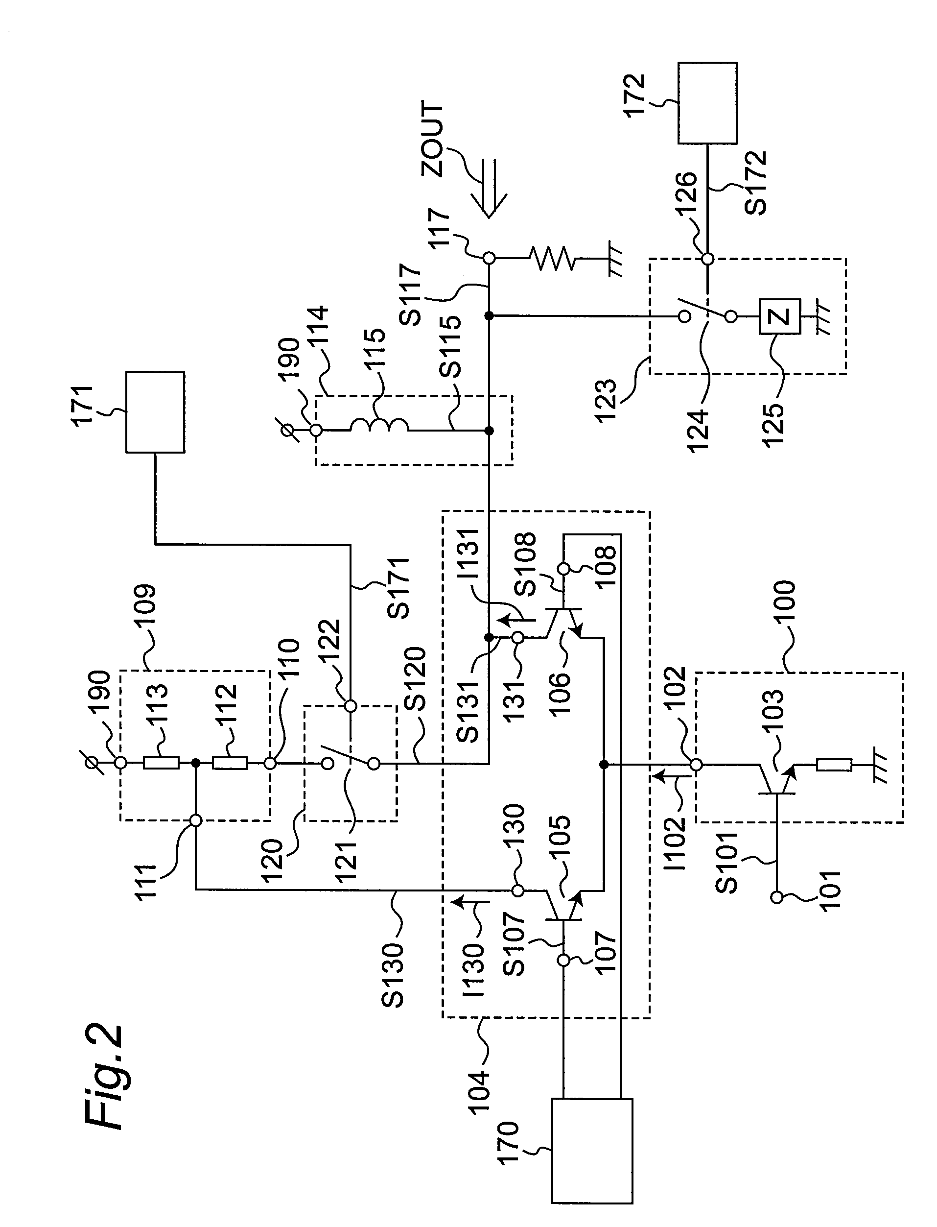
[0072]FIG. 2 is a circuit diagram of an amplifier circuit according to a second embodiment of the invention. Compared with the amplifier circuit of the first embodiment, this embodiment additionally has a variable impedance circuit 123 connected between the collector 131 of the gain control circuit 104 and the output pin 117.

[0073]The variable impedance circuit 123 has an impedance device 125 with a predetermined impedance, and a switch 124 that turns on / off electrically based on a control signal S172 applied from a control signal generating circuit 172.

[0074]In general, high frequency signals used for wireless communication have an extremely short wavelength, and some measures of reducing signal loss...

embodiment 3

[0088]A third embodiment of the invention is described next focusing on the differences with the first and second embodiments. Other aspects of the arrangement, operation, and effect of the third embodiment are the same as in the first and second embodiments, and further description thereof is omitted below.

[0089]FIG. 10 is a circuit diagram of an amplifier circuit according to a third embodiment of the invention. Compared with the amplifier circuit of the first embodiment, this embodiment additionally has a bypass circuit 150 inserted between the input pin 101 and output pin 117. The bypass circuit 150 has a switch 152 that switches on / off according to the control signal S175 input from the control signal generating circuit 175, and a capacitor 151 used to cut the dc voltage from the input pin 101.

[0090]Wireless communication devices are designed to be carried around freely and at times are used near the communication base station. Because signals significantly exceeding the limite...


PUM


Abstract

An amplifier circuit has a current conversion circuit that receives a high frequency signal and produces a signal current according to the high frequency signal; a gain control circuit that includes a control signal input for receiving a control signal, a first output, and a second output, and produces the signal current from the first output or the second output according to the control signal; an impedance circuit that includes a first node connected to the first output, a second node connected to the second output, and a third node, the impedance circuit presenting a predetermined impedance between the nodes; a switch circuit that is inserted between the first output and the first node; and a load impedance unit that is connected to the first output and produces a gain signal representing an amplified high frequency signal.

Description

BACKGROUND OF THE INVENTION[0001]1. Field of Invention[0002]The present invention relates to technology for an amplifier circuit used in the receiver of a wireless communication device such as a cell phone or PHS phone, and relates more particularly to an amplifier circuit and a wireless communication device.[0003]2. Description of Related Art[0004]A variable gain amplifier according to the prior art is shown in FIG. 11. In FIG. 11 a high frequency signal S201 is input to a current conversion circuit 200 through an input node 201. The high frequency signal S201 is input to the base of a transistor 203, and a signal current I202 corresponding to the high frequency signal S201 is then output through the collector of the transistor 203 from the output node 202 of the current conversion circuit 200.[0005]The signal current I202 is then input to a gain control circuit 204 connected in common to the output node 202. The gain control circuit 204 consists of transistors 205 and 206 having t...

Claims


Application Information

Patent Timeline
Patent Type & Authority Patents(United States)
IPC IPC(8): H03G3/10
CPCH03G1/0088
Inventor OKAMOTO, NAOKIKOHAMA, HIROYUKISHIBATA, MAKI
Owner COLLABO INNOVATIONS INC
Learn More