Coreless cavity substrates for chip packaging and their fabrication

a cavity substrate and chip packaging technology, applied in the direction of photomechanical equipment, printed circuit non-printed electric components association, instruments, etc., can solve the problems of inherently expensive connection technology, time-consuming, expensive and inefficient, and shorten the time-to-market of connection technology, etc., and achieve high yield

Active Publication Date: 2010-03-02
ZHUHAI ADVANCED CHIP CARRIERS & ELECTRONICS SUBSTRATE SOLUTIONS TECH
View PDF1 Cites 147 Cited by
  • Summary
  • Abstract
  • Description
  • Claims
  • Application Information

AI Technical Summary

Benefits of technology

[0038]It is an aim to provide a manufacturing technique that attains high yields.
[0039]It is a further aim of the invention to provide a manufacturing route for a compact, reliable packaging support for two or more IC chips that is economical and is particularly suitable for large scale manufacture.

Problems solved by technology

As the IC of such products becomes ever more complex, the IC package continually requires more interconnections (pins or leads) with its surroundings to support increased logic and power requirements.
This approach not only allows cost reduction of the complex IC but typically shortens their time-to-market as well.
This requires holes to be drilled through the substrate, one at a time, in a stepwise manner, and is thus very time-consuming, expensive and inefficient.
It will be appreciated however, that such a connection technology is inherently expensive as each via is required to be drilled and then filled, and the drilling has to be done one via at a time, stepwise.
This makes production time consuming and hence, expensive.
This results in ceramic chip carriers exhibiting relatively low signal propagation speeds in comparison to substrates of other materials, particularly those with organic components, such as fiberglass-reinforced epoxy resin, polytetrafluoroethylene (Teflon), and the like.
These techniques are characterized by poor dimensional accuracy and low precision.
Such a connection technology is inherently expensive as each via is required to be drilled and then filled, and the drilling has to be performed stepwise, one via at a time.
This makes production time-consuming and hence, expensive.
This approach will, of necessity, result in a relatively thick stack.
The formation of vias and cavities one at a time in this manner is time consuming and hence, expensive.
For mass production, where many packages are fabricated at once, such techniques are inherently unsuitable.

Method used


Image

  • Coreless cavity substrates for chip packaging and their fabrication
  • Coreless cavity substrates for chip packaging and their fabrication
  • Coreless cavity substrates for chip packaging and their fabrication

Examples


Embodiment Construction

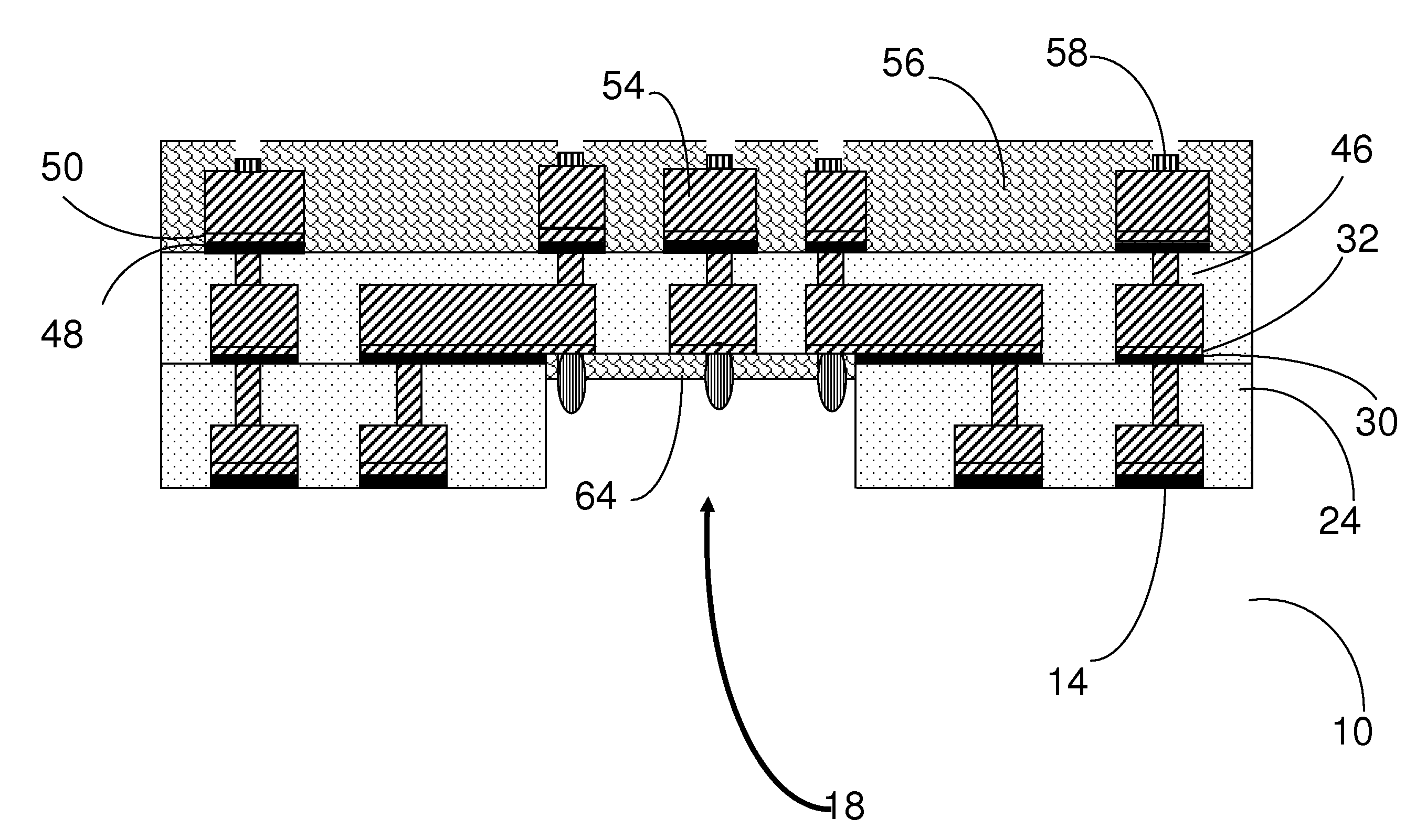
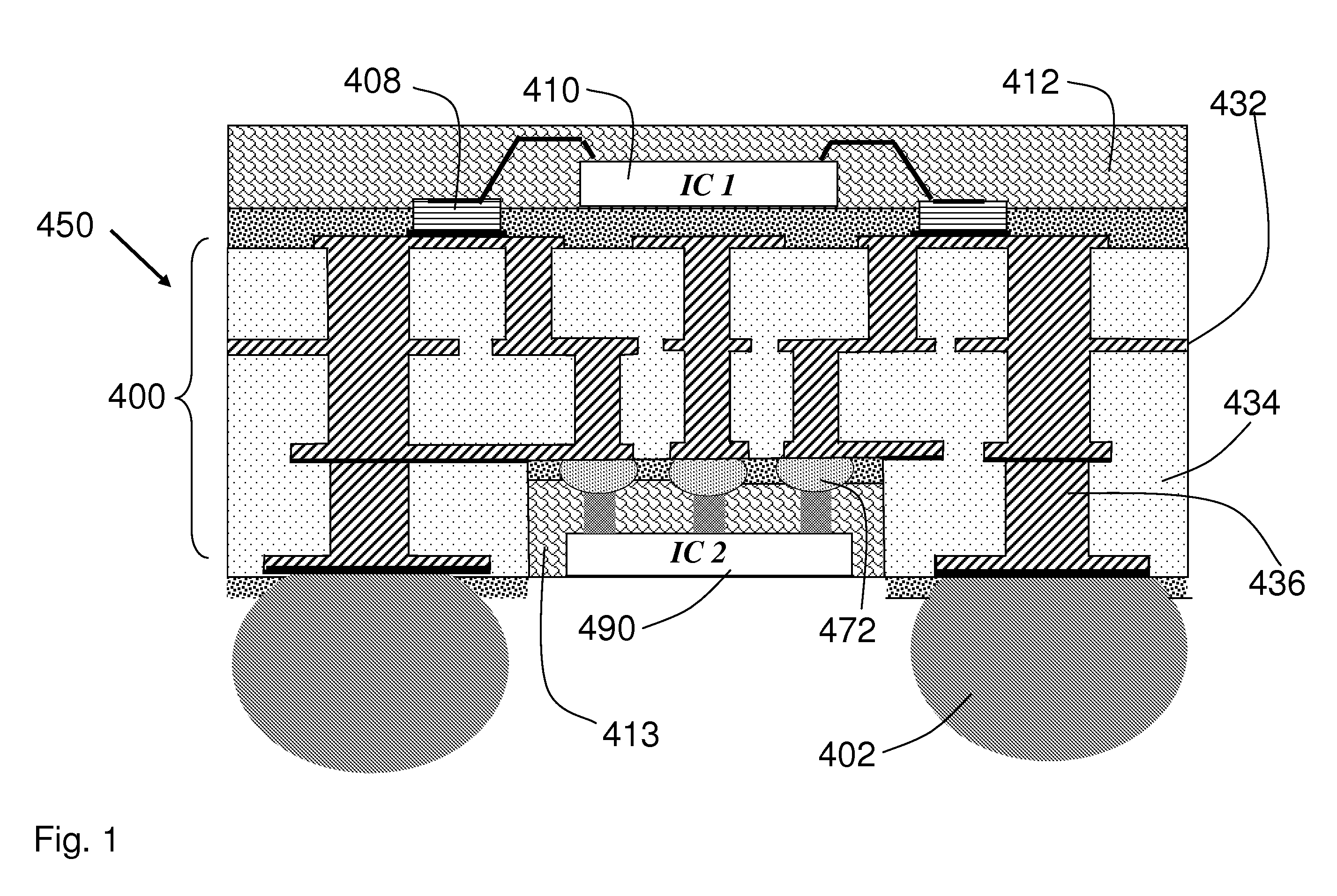
[0088]With reference to FIG. 1, the present invention relates to a compact, reliable packaging 450 for two IC chips 410, 490, and particularly to a coreless IC support substrate 400 having dimensions of, say, 14 mm×14 mm, and a thickness of less than 1 mm, and having a cavity therein of, say, 9 mm×9 mm×0.1 mm, such that a first IC 410, such as a memory die for example, may be wire bonded or otherwise attached to the Ni / Au terminations 408 on the top side of the IC support substrate 400 thus formed, and a second IC 490 may be connected within the cavity 480, by a ball grid array or a land grid array of solder bumps 472. Applying terminations such as solder balls 402, over outer vias 436 of the packaging support substrate 400 provides a compact packaging 450, which, by stacking one IC chip 410 onto the other 490, is space conserving, enabling further miniaturization of, for example, flash memory devices such as the so-called, disk-on-keys and MP3 devices, and mobile phones and the lik...


PUM

PropertyMeasurementUnit
temperatureaaaaaaaaaa
concentrationaaaaaaaaaa

Abstract

A method for fabricating an IC support for supporting a first IC die connected in series with a second IC die; the IC support comprising a stack of alternating layers of copper features and vias in insulating surround, the first IC die being bondable onto the IC support, and the second IC die being bondable within a cavity inside the IC support, wherein the cavity is formed by etching away a copper base and selectively etching away built up copper.

Description

FIELD OF THE INVENTION[0001]The present invention is directed to providing coreless cavity substrates for packaging integrated circuits, and to methods for the manufacture thereof.BACKGROUND[0002]Electronic products in general and mobile devices in particular, have revolutionized the world over the past few decades with laptop computers, palm computers, wireless phones, digital cameras, to name just a few electronic products developed in recent years. Subsequent generations of such products are ever more compact, with improved features and functions. The integrated circuit (IC) and the more efficient packaging of the IC have played pivotal roles in enhancing the functionality and further miniaturization of these products.[0003]As the IC of such products becomes ever more complex, the IC package continually requires more interconnections (pins or leads) with its surroundings to support increased logic and power requirements. At the same time, the IC package is required to be ever sma...

Claims


Application Information

Patent Timeline
Patent Type & Authority Patents(United States)
IPC IPC(8): H05K3/10H01R12/50
CPCH01L21/4857H01L23/13H01L23/49822H05K1/183H05K3/4647H05K3/4682H05K3/4697Y10T29/49117H01L2221/68345H01L2224/16225H01L2224/48095H01L2224/48227H01L2924/0102H01L2924/01078H01L2924/01079H01L2924/09701H01L2924/15153H01L2924/1517H01L2924/15311H01L2924/1532H01L2924/19041H01L2924/30107H05K3/06H05K3/205H05K2203/0733H01L24/48H01L2924/01019H01L2924/10253H01L21/4864Y10T29/49121H01L2224/16235Y10T29/49155Y10T29/49156Y10T29/49128Y10T29/49147H01L2924/00H01L2924/12042H01L2924/181H01L2924/14H01L2924/00014H01L2924/00012H01L2224/45099H01L2224/45015H01L2924/207
Inventor HURWITZ, DRORFARKASH, MORDECHAYIGNER, EVASTATNIKOV, BORISMICHAELI, BENNY
Owner ZHUHAI ADVANCED CHIP CARRIERS & ELECTRONICS SUBSTRATE SOLUTIONS TECH
Why Eureka
Try Eureka