
Three-dimensional metal microfabrication process and devices produced thereby

a three-dimensional metal and micro-fabrication technology, applied in the field of three-dimensional metal micro-fabrication process and the production of thereby, can solve the problems of increasing cost, complicating processing, and microelectronics-based metallic micromachining techniques that do not provide the same degree of design freedom as conventional multi-axis micromachining techniques, etc., to simplify the timing of such process, simplify the fabrication of metallic micro-scale structures, and simplify the effect of surface height profiles

Active Publication Date: 2010-03-23
RGT UNIV OF CALIFORNIA
View PDF5 Cites 3 Cited by
  • Summary
  • Abstract
  • Description
  • Claims
  • Application Information

AI Technical Summary

Benefits of technology

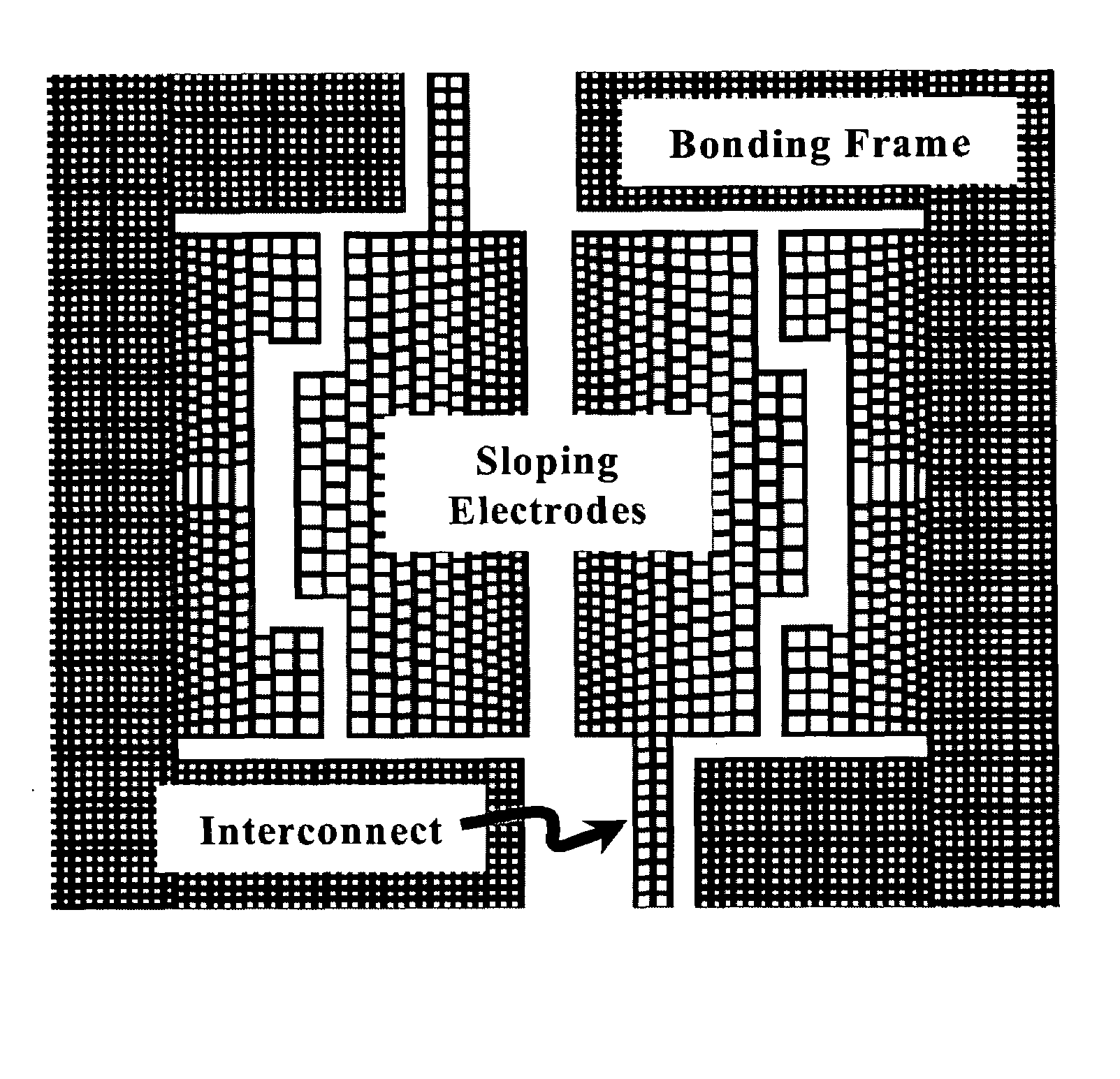
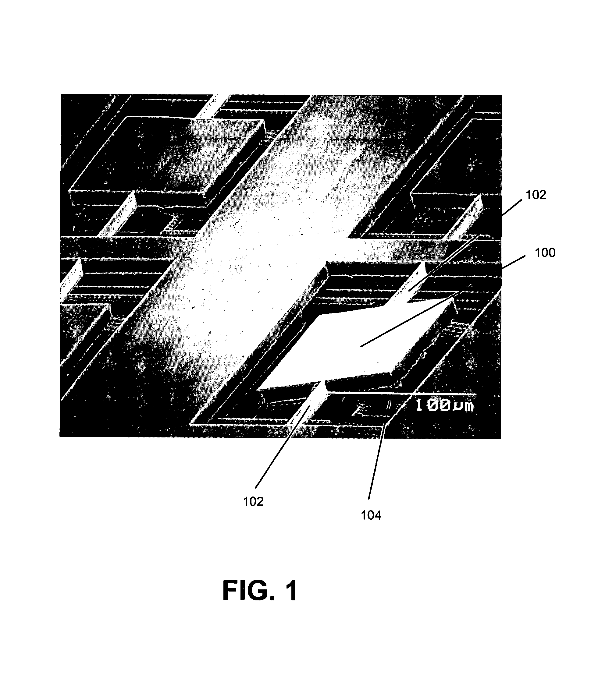
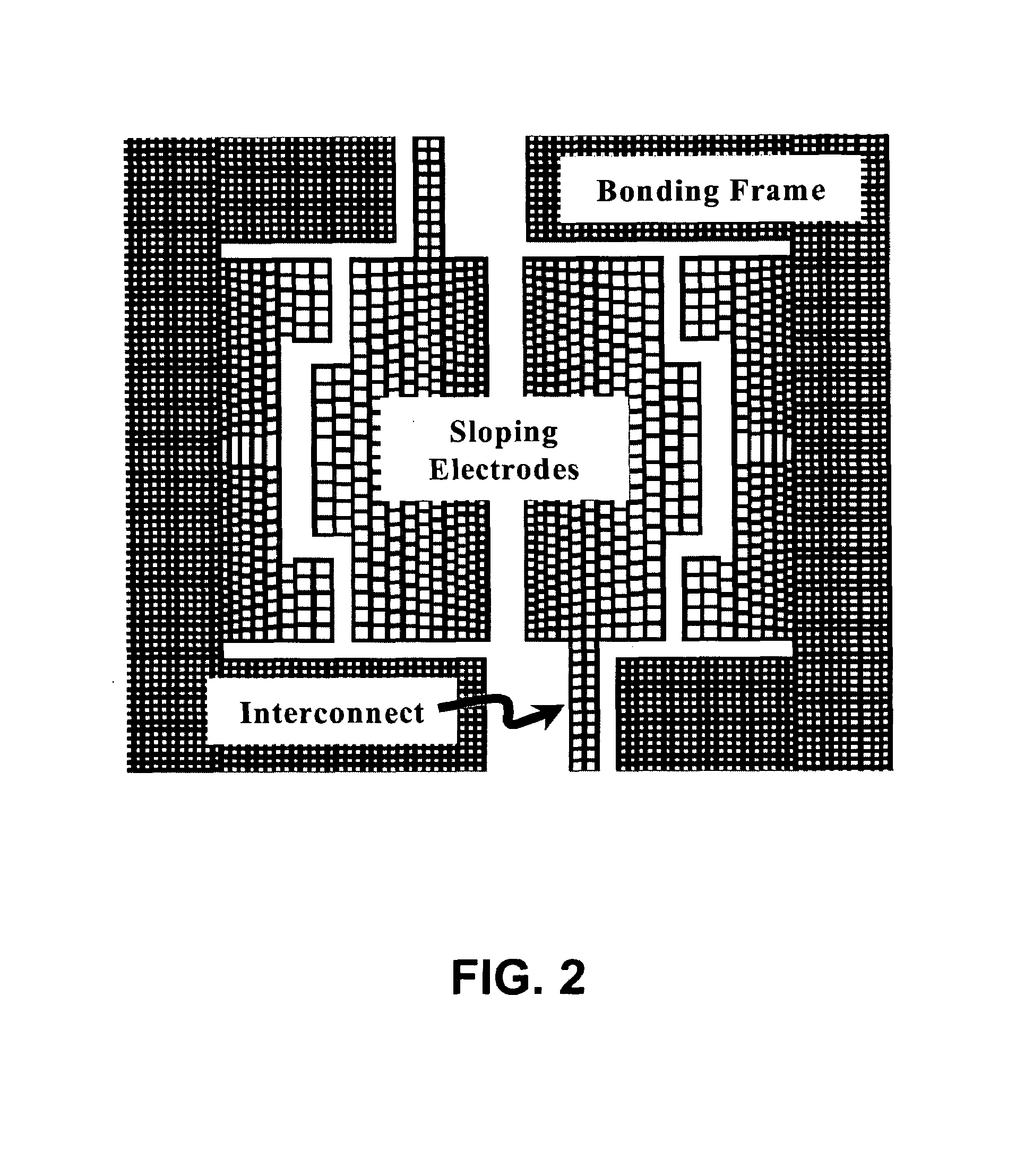
The present invention is about a process for making metallic micro-scale structures with complex surface height profiles. It uses a photolithographic etch mask with multiple openings to modulate the etch depths and remove the superstructure above the etched floors. This simplifies the fabrication process and reduces the impact on other structures in the device. The method can create structures with multiple height levels, non-planar surfaces, and electrically active surfaces. The device can be a microactuator, microsensor, microtransducer, or microstructure. The invention also includes a microdevice with sloping electrodes underneath it, which have a smaller gap distance near the center to reduce the required drive voltage. The sloping electrodes have a stepwise linear profile generated by selecting the size, shape, and pitch of the etching opening. The method can be performed with a single lithographic patterning step and can make use of the poor coverage conformality of e-beam deposition.

Problems solved by technology

Microelectronics-based metallic micromachining techniques, however, do not provide the same degree of design freedom as conventionally-based multi-axis micromachining techniques.
Greater structural complexity can be achieved with additional photolithographic patterning steps, bonding of additional substrates, and / or use of sacrificial layers, but this often complicates processing and therefore increases cost and reduces yield considerably.

Method used


Image

  • Three-dimensional metal microfabrication process and devices produced thereby
  • Three-dimensional metal microfabrication process and devices produced thereby
  • Three-dimensional metal microfabrication process and devices produced thereby

Examples


Embodiment Construction

[0027]In the following description of the preferred embodiment, reference is made to the accompanying drawings that form a part hereof, and in which is shown by way of illustration a specific embodiment in which the invention may be practiced. It is to be understood that other embodiments may be utilized and structural changes may be made without departing from the scope of the present invention.

Technical Description

[0028]The recent development of highly anisotropic metal bulk micromachining processes has provided the opportunity for extension of metal microfabrication capability well into the third dimension [1]. While this capability has enabled fabrication of complex, high aspect ratio structures, these structures are generally simple, prismatic, 3-D projections of the planar mask pattern used to define them. For some applications, however, truly 3-D structures are desired, especially those that posses arbitrary surface height profiles, i.e. surfaces with multiple height levels a...


PUM

PropertyMeasurementUnit
sizeaaaaaaaaaa
sizeaaaaaaaaaa
etch ratesaaaaaaaaaa

Abstract

The present invention relates, in general, to a method for three-dimensional (3D) microfabrication of complex, high aspect ratio structures with arbitrary surface height profiles in metallic materials, and to devices fabricated in accordance with this process. The method builds upon anisotropic deep etching methods for metallic materials previously developed by the inventors by enabling simplified realization of complex, non-prismatic structural geometries composed of multiple height levels and sloping and / or non-planar surface profiles. The utility of this approach is demonstrated in the fabrication of a sloping electrode structure intended for application in bulk micromachined titanium micromirror devices, however such a method could find use in the fabrication of any number of other microactuator, microsensor, microtransducer, or microstructure devices as well.

Description

CROSS-REFERENCE TO RELATED APPLICATIONS[0001]This application claims benefit under 35 U.S.C §119(e) of the following and commonly-assigned provisional application:[0002]Application Ser. No. 60 / 686,409, entitled “THREE-DIMENSIONAL MICROFABRICATION PROCESS AND DEVICES PRODUCED THEREBY,” filed on Jun. 2, 2005, by Masaru P. Rao, Marco F. Aimi, and Noel C. MacDonald, which application is incorporated by reference herein.STATEMENT REGARDING FEDERALLY SPONSORED RESEARCH AND DEVELOPMENT[0003]This invention was made with Government support under Grant No. W9113M-04-01-0001 awarded by the Army Research Office, and Grant Nos. W9113M-04-01-D001 awarded by DARPA. The Government has certain rights in this invention.BACKGROUND OF THE INVENTION[0004]1. Field of the Invention[0005]The present invention is related to metallic micromechanical materials, methods, and devices, and more particularly, to the fabrication of three-dimensional metallic micromechanical devices.[0006]2. Description of the Rela...

Claims


Application Information

Patent Timeline
Patent Type & Authority Patents(United States)
IPC IPC(8): H01L21/3205H01L21/4763
CPCC23F4/00B81C1/00126B81B2201/042B81B2203/033Y10T29/49117B81C2201/0132
Inventor RAO, MASARU P.AIMI, MARCO F.MACDONALD, NOEL C.
Owner RGT UNIV OF CALIFORNIA
Learn More