Semiconductor device

a technology of electromagnetic radiation and semiconductors, applied in the structure of radiating elements, resonant antennas, protective materials, etc., can solve the problems of short communication distance, limited size or shape of each antenna, and difficulty in disconnection, so as to reduce the communication distance from the communication device.

Inactive Publication Date: 2010-03-23
SEMICON ENERGY LAB CO LTD
View PDF7 Cites 28 Cited by
  • Summary
  • Abstract
  • Description
  • Claims
  • Application Information

AI Technical Summary

Benefits of technology

[0008]In view of the foregoing problems, an object of the present invention is to provide a semiconductor device in which even in the case where a plurality of antennas are provided, there is no limitation on the layout of the antennas so that disconnection between an integrated circuit portion and the antennas and reduction in a communication distance from a communication device can be prevented.
[0009]A semiconductor device of the present invention includes an integrated circuit portion and a plurality of antennas. The size of the integrated circuit portion can be almost the same as a desired antenna size, the integrated circuit portion and the antennas can be easily connected, and signal transmission and reception with a communication device can be reliably performed. A specific structure is described below.
[0017]Note that in the present invention, various types of transistors can be applied to a transistor. Therefore, types of transistors which can be applied are not limited to a certain type. For example, a thin film transistor (TFT) including a non-single crystalline semiconductor film typified by amorphous silicon or polycrystalline silicon can be applied. A transistor or the like formed by an ink-jet method or a printing method may also be employed. With use of them, such transistors can be manufactured at a room temperature, can be manufactured at a low vacuum, and can be manufactured using a large substrate. In addition, since such transistors can be manufactured without use of a mask (reticle), the layout of the transistors can be easily changed. A transistor including an organic semiconductor or a carbon nanotube, or other transistors can be applied as well. With use of them, the transistors can be formed over a substrate which can be bent. Note that a non-single crystalline semiconductor film may include hydrogen or halogen. In addition, various types of substrates can be applied to a substrate provided with transistors are formed without limitation to a certain type.
[0018]A transistor can have various structures without limitation to a certain structure. For example, a multi-gate structure having two or more gate electrodes may be used. With the multi-gate structure, channel regions are connected in series; therefore, a plurality of transistors are connected in series. With the multi-gate structure, an off current can be reduced, and the withstand voltage of the transistor can be increased, which improves reliability. In addition, even if a drain-source voltage fluctuates when. the transistor operates in a saturation region, drain-source current does not fluctuate very much, and stable characteristics can be provided. In addition, a structure in which gate electrodes are formed above and below a channel may be used. With the use of the structure in which gate electrodes are formed above and below the channel, a channel region is enlarged so that the amount of current flowing therethrough is increased, or a depletion layer can be easily formed, so that the subthreshold swing is decreased. Further, when the gate electrodes are provided above and below the channel, a plurality of transistors are connected in parallel.
[0019]Further, a gate electrode may be provided above or below the channel. Either a staggered structure or an inversely staggered structure may be employed. A channel region may be divided into a plurality of regions, or connected in parallel or in series. Further, a source electrode or a drain electrode may overlap with a channel (or a part of it), thereby preventing a charge from being accumulated in a part of the channel and being unstable operation. Further, an LDD region may be provided. By providing an LDD region, an off current can be reduced and reliability can be improved by improving the withstand voltage of a transistor, and further stable characteristics can be obtained since a drain-source current does not change so much even when a drain-source voltage changes in the operation in a saturation region.
[0021]According to the present invention, even in the case where a plurality of antennas are provided, there is no limitation on the layout of the antennas and thus the antennas can have desired shapes. Further, disconnection between the antenna and an integrated circuit portion and reduction in a communication distance from a communication device can be prevented.

Problems solved by technology

However, in a case where a plurality of antennas are provided on one surface in a semiconductor device including the plurality of antennas, there is a possibility that the size or the shape of each antenna are limited because of limitation on the layout of the antennas and thus a communication distance is short.
Further, in a case where a plurality of antennas are formed over different substrates and attached to a fine chip provided with an integrated circuit portion, disconnection is a problem.
However, an on-chip antenna which is formed in a fine chip causes problems that the size of the antenna is reduced and a communication distance is shortened.
Although it is possible that the size of a chip formed of a silicon substrate is increased in order that disconnection and reduction in a communication distance may be prevented, there are problems such as increase in cost and damage of the silicon chip.

Method used


Image

  • Semiconductor device
  • Semiconductor device
  • Semiconductor device

Examples


embodiment mode 1

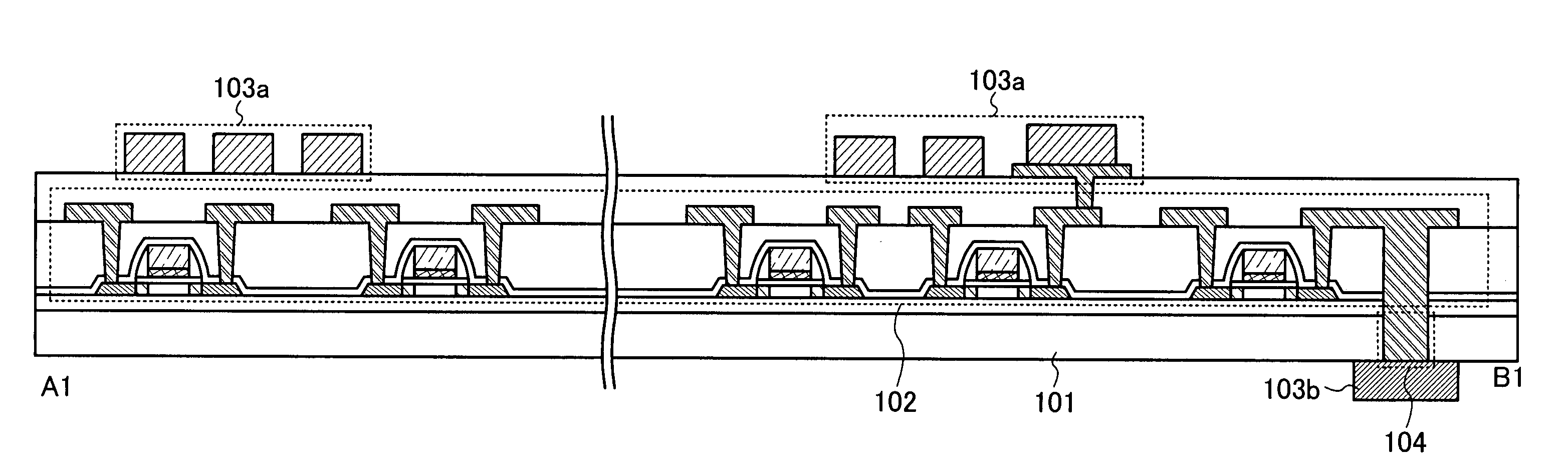
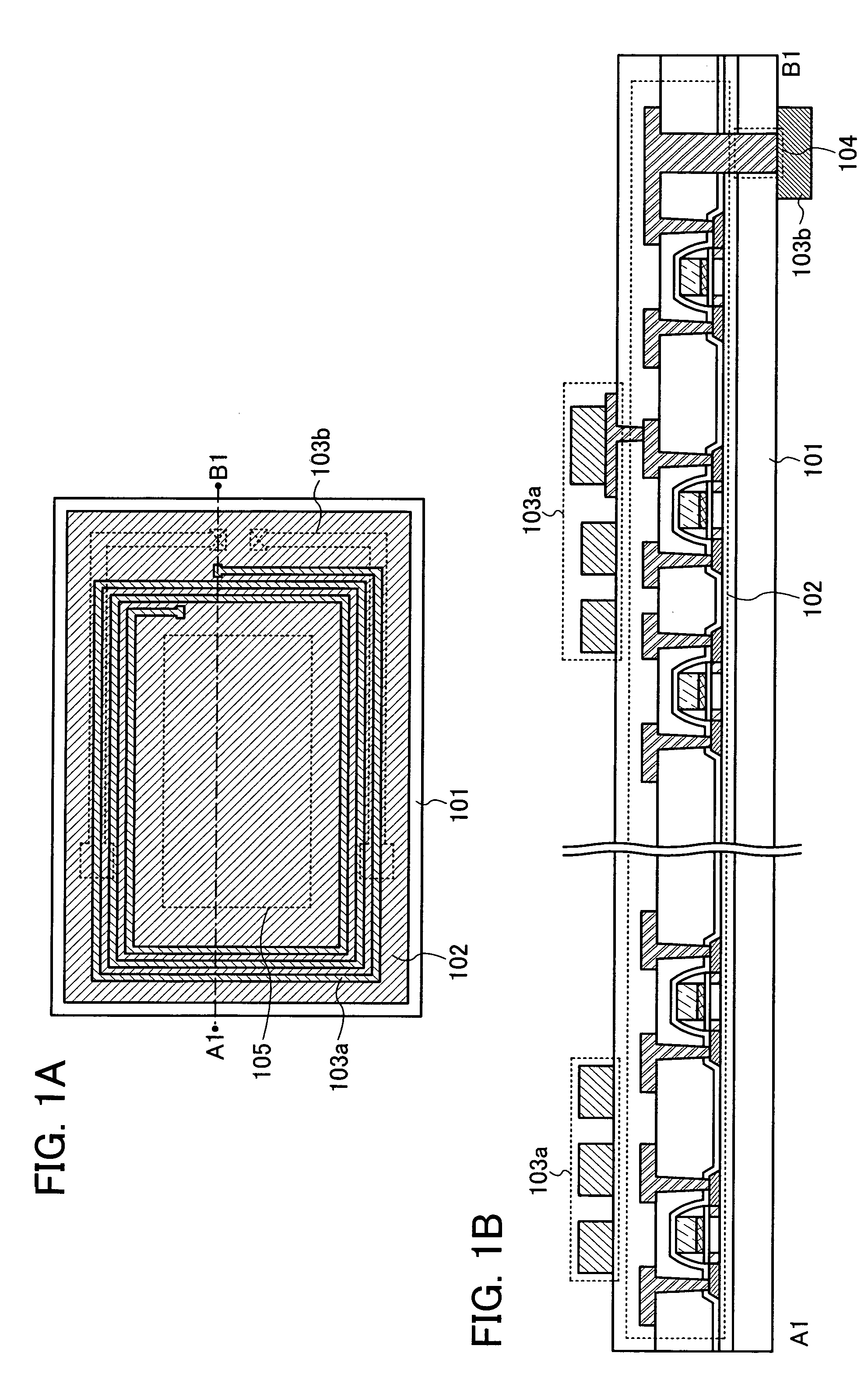
[0044]A semiconductor device of the present invention includes a plurality of antennas provided on different surfaces, in which antennas provided on at least one surface are on-chip antennas formed over an integrated circuit portion. A structure including a plurality of antennas provided on two different surfaces, in which antennas provided on one surface are on-chip antennas formed in the same step as an integrated circuit, is described below with reference to FIGS. 1A and 1B. Note that FIG. 1A is a schematic top view of a semiconductor device and FIG. 1B is a schematic cross-sectional view along line A1-B1 in FIG. 1A.

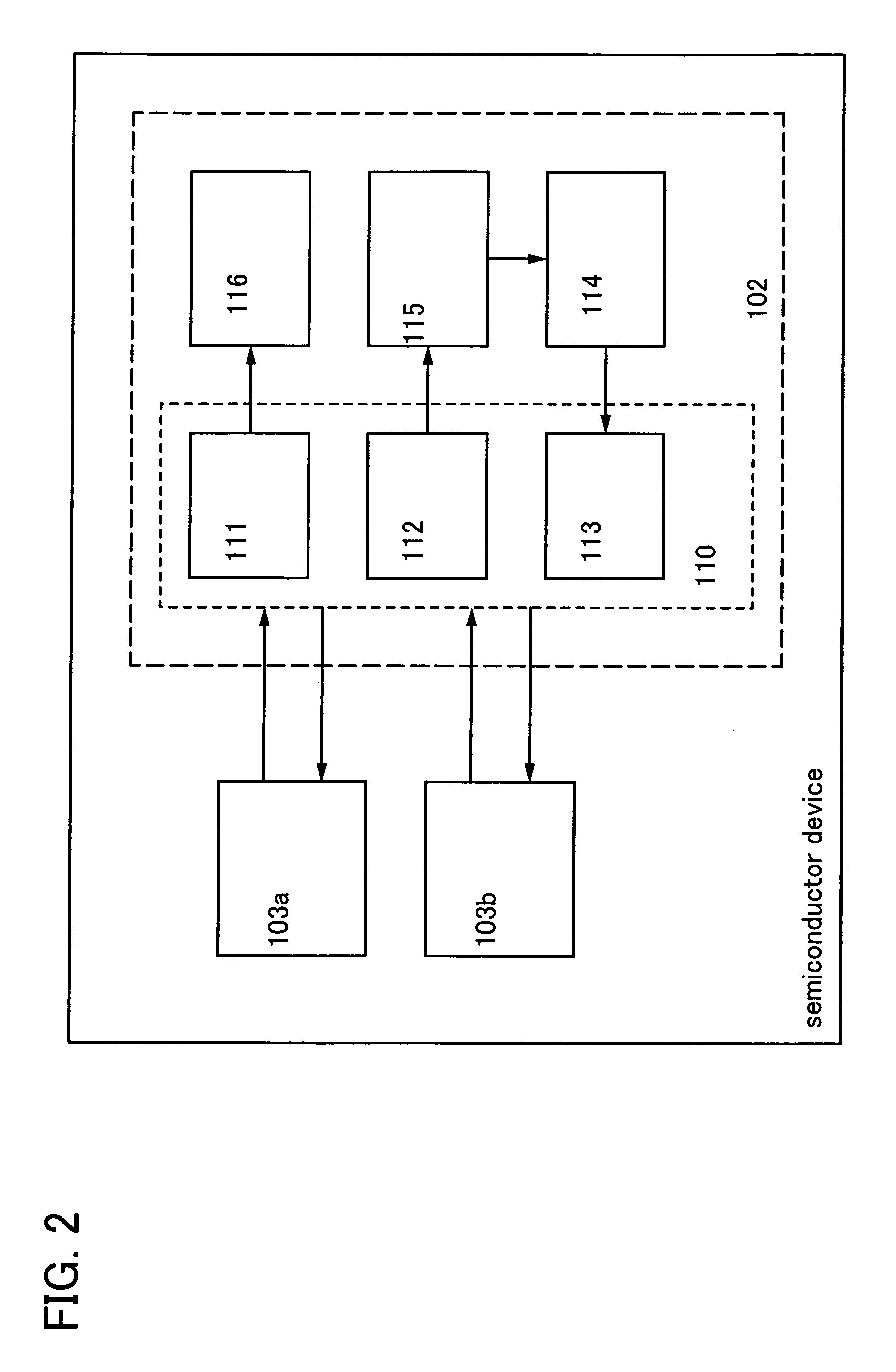
[0045]The semiconductor device described in this embodiment mode includes an integrated circuit portion 102 which is provided on a first surface (hereinafter also referred to as one surface) of an insulating base (here, a substrate 101), a first antenna 103a which is provided over the integrated circuit portion 102, and a second antenna 103b which is provided over a s...

embodiment mode 2

[0067]In this embodiment mode, the structure of a semiconductor device different from that of Embodiment Mode 1 is described with reference to the drawings. Note that FIG. 4A is a schematic top view of the semiconductor device and FIG. 4B is a schematic cross-sectional view along line A1-B1 in FIG. 4A.

[0068]The semiconductor device described in this embodiment mode includes the integrated circuit portion 102 which is provided on a first surface (one surface) of the substrate 101, the first antenna 103a which is provided over the integrated circuit portion 102, and the second antenna 103b which is provided over a second surface (the other surface) of the substrate 101 (see FIGS. 4A and 4B). The integrated circuit portion 102 includes a first integrated circuit portion 102a and a second integrated circuit portion 102b which are connected to the first antenna 103a and the second antenna 103b, respectively.

[0069]The first antenna 103a is an on-chip antenna which is formed so as to be el...

embodiment mode 3

[0077]In this embodiment mode, the structure of a semiconductor device different from those of Embodiment Modes 1 and 2 is described with reference to the drawings. Note that FIG. 7A is a schematic top view of a semiconductor device and FIG. 7B is a schematic cross-sectional view along line A1-B1 in FIG. 7A.

[0078]The semiconductor device described in this embodiment mode includes the integrated circuit portion 102 which is provided on a first surface (one surface) of the substrate 101, the first antenna 103a which is provided over the integrated circuit portion 102, a third antenna 103c which is provided over the first antenna 103a, and the second antenna 103b which is provided on a second surface (the other surface) of the substrate 101 (see FIGS. 7A and 7B). Here, a case is shown in which the first antenna 103a and a wiring 134 which is electrically connected to a thin film transistor included in the integrated circuit portion 102 are provided on one surface.

[0079]The first antenn...


PUM


Abstract

An object is to provide a semiconductor device in which even in the case where a plurality of antennas are provided, there is no limitation on the layout of the antennas so that disconnection between an integrated circuit portion and the antenna and reduction in a communication distance from a communication device can be prevented. An integrated circuit portion which includes a thin film transistor is provided on a first surface of an insulating base. A first antenna is provided over the integrated circuit portion. A second antenna is provided over a second surface of the base. The first antenna is connected to the integrated circuit potion. The second antenna is connected to the integrated circuit portion through a through hole formed in the base. The first antenna and the second antenna overlap with the integrated circuit portion.

Description

BACKGROUND OF THE INVENTION[0001]1. Field of the Invention[0002]The present invention relates to a semiconductor device, and particularly relates to a semiconductor device which performs wireless communication by using electromagnetic waves.[0003]2. Description of the Related Art[0004]In recent years, an individual identification technology using electromagnetic waves for wireless communication has attracted attention. In particular, as a semiconductor device which communicates data by wireless communication, an individual identification technology using a semiconductor device (also referred to as an RFID tag, an IC (integrated circuit) tag, an IC chip, an RF tag, a wireless tag, or an electronic tag) utilizing RFID (radio frequency identification) has attracted attention. The individual identification technology using such a semiconductor device utilizing RFID has been useful for production, management, or the like of an individual object, and application to personal authentication...

Claims


Application Information

Patent Timeline
Patent Type & Authority Patents(United States)
IPC IPC(8): H01Q1/38
CPCH01Q1/2225H01Q1/2283
Inventor KOYAMA, JUNYAMAZAKI, SHUNPEI
Owner SEMICON ENERGY LAB CO LTD
Why Eureka
Try Eureka