Methods for manufacturing RFID tags and structures formed therefrom

a technology of radio frequency identification and manufacturing methods, applied in the direction of burglar alarm mechanical actuation, burglar alarm by hand-portable object removal, etc., can solve the problem that the dividing down carrier frequency directly requires ghz-speed clocking circuit and its associated energy loss, and achieves low cost, cost-effectiveness, and low cost

Active Publication Date: 2010-03-30
ENSURGE MICROPOWER ASA
View PDF40 Cites 29 Cited by
  • Summary
  • Abstract
  • Description
  • Claims
  • Application Information

AI Technical Summary

Benefits of technology

[0020]The present invention provides a way to integrate liquid Si deposition into a cost effective, integrated manufacturing process for the manufacture of RFID circuits. Many of the active semiconductor components, including diodes and transistors, are thin film-based. Based on the demonstrated performance of Si ink-derived semiconductor films, in terms of such parameters as mobility, doping / carrier concentration, and other parameters, functional RFID tags in the LF, HF, UHF, and microwave carrier frequency regimes are possible. The present thin film approach utilizing Si ink is attractive as this can be done at relatively low cost per unit area which further enables low cost, relatively large die which can be inexpensively integrated directly on antennae and / or inexpensively and quickly attached to antennae using processes such as conductive adhesive and crimp bonding. Furthermore, the present RFID tags generally provide higher performance (e.g., improved electrical characteristics) as compared to tags containing organic electronic devices.
[0026]Selection of a stainless steel substrate sealed and / or coated with an insulator (e.g., printed or conventionally deposited spin-on glass [SOG], or a CVD oxide and / or nitride), allowing the use of both furnace based crystallization as well as thermal oxidation of Si for the formation of high mobility and / or high conductivity silicon and gate oxide(s), respectively;
[0027]Elongated (lateral) contacts to the lower electrode of the diode, placed relatively close to an elongated active region, thereby limiting the series resistance between the metallic contacts to the diode, allowing for a simpler and lower cost overall integration;
[0028]A heavily doped bottom contact / interconnect layer for diodes, to eliminate the need for an additional metal interconnect layer and enable simultaneous growth of a capacitor dielectric layer (the diodes can optionally be either p- or n- / metal Schottky diodes or p / n diodes);
[0034]A single metal interconnect layer for many different components of the circuit (metal substrate dipole contact, gate conductor contact for interconnect and capacitors, Si contact for diodes, and contacts to transistor source / drain terminals), reducing the total number of metal layers (and therefore the process cost, although one should carefully design a layout, integration / manufacturing process and via / interlayer dielectric [ILD] / metallization process that provide a suitable circuit topography and that are compatible with each other; e.g., in the case of a layout that includes formation of Schottky contacts, a common metallization such as Ti / Al may serve as both interconnect and the Schottky metal where it contacts undoped or lightly doped semiconductor layers); and

Problems solved by technology

Also, dividing down the carrier frequency directly requires GHz-speed clocking circuits and their associated energy losses.

Method used


Image

  • Methods for manufacturing RFID tags and structures formed therefrom
  • Methods for manufacturing RFID tags and structures formed therefrom
  • Methods for manufacturing RFID tags and structures formed therefrom

Examples


Embodiment Construction

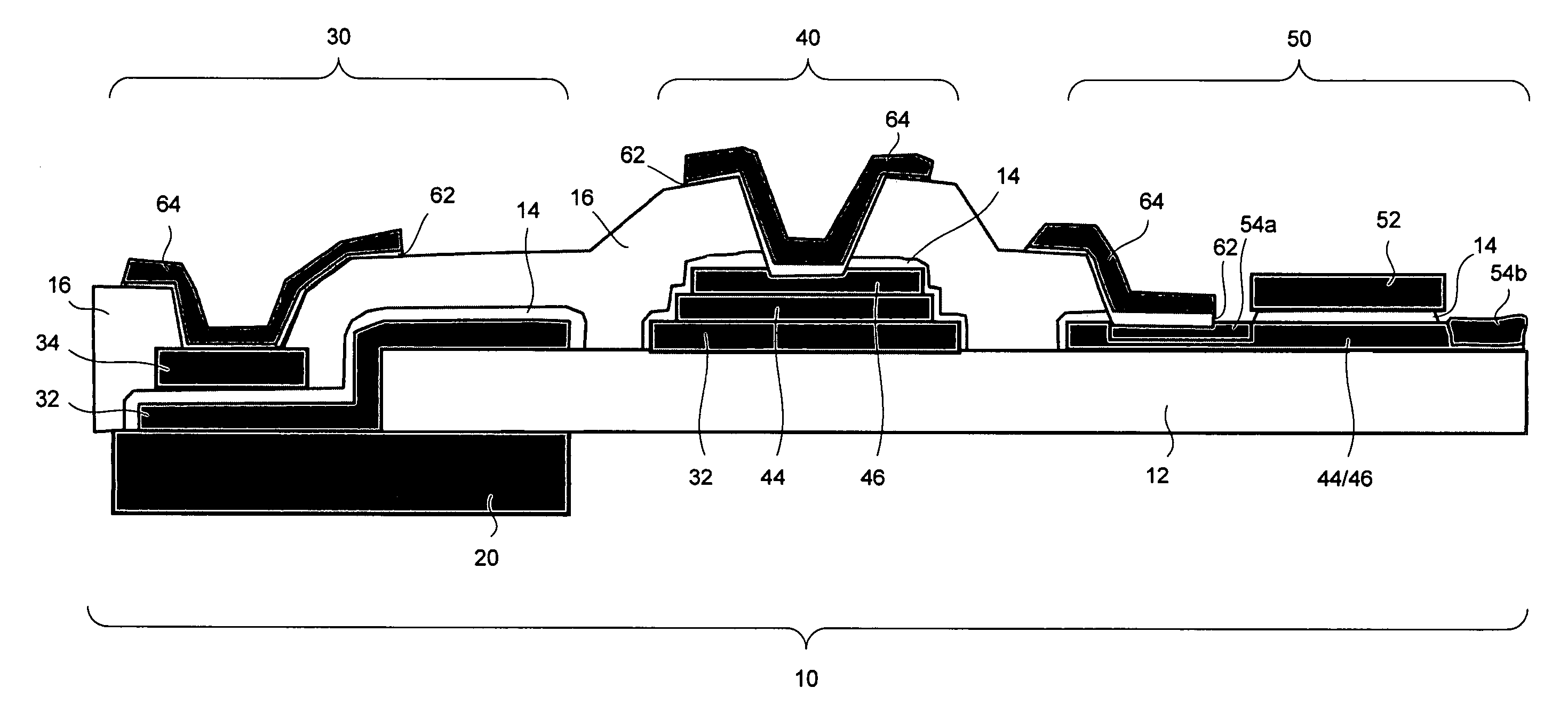
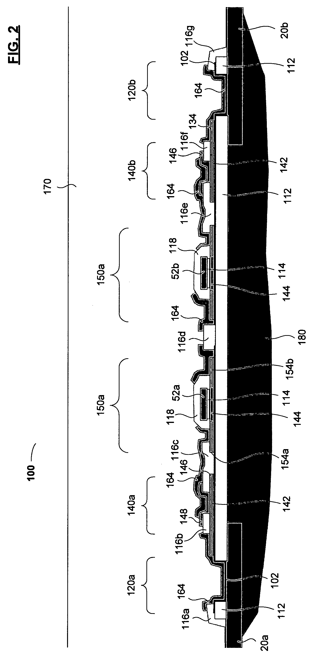
[0049]Reference will now be made in detail to the preferred embodiments of the invention, examples of which are illustrated in the accompanying drawings. While the invention will be described in conjunction with the preferred embodiments, it will be understood that they are not intended to limit the invention to these embodiments. On the contrary, the invention is intended to cover alternatives, modifications and equivalents, which may be included within the spirit and scope of the invention. Furthermore, in the following detailed description of the present invention, numerous specific details are set forth in order to provide a thorough understanding of the present invention. However, it will be readily apparent to one skilled in the art that the present invention may be practiced without these specific details. In other instances, well-known methods, procedures, components, and circuits have not been described in detail so as not to unnecessarily obscure aspects of the present inv...


PUM


Abstract

Radio frequency identification (RFID) tags and processes for manufacturing the same. The RFID device generally includes (1) a metal antenna and / or inductor; (2) a dielectric layer thereon, to support and insulate integrated circuitry from the metal antenna and / or inductor; (3) a plurality of diodes and a plurality of transistors on the dielectric layer, the diodes having at least one layer in common with the transistors; and (4) a plurality of capacitors in electrical communication with the metal antenna and / or inductor and at least some of the diodes, the plurality of capacitors having at least one layer in common with the plurality of diodes and / or with contacts to the diodes and transistors. The method preferably integrates liquid silicon-containing ink deposition into a cost effective, integrated manufacturing process for the manufacture of RFID circuits. Furthermore, the present RFID tags generally provide higher performance (e.g., improved electrical characteristics) as compared to tags containing organic electronic devices.

Description

RELATED APPLICATIONS[0001]This application claims the benefit of U.S. Provisional Application No. 60 / 697,599, filed Jul. 8, 2005, incorporated herein by reference in its entirety.FIELD OF THE INVENTION[0002]The present invention generally relates to the field of radio frequency identification (RFID) tags and processes for manufacturing the same.BACKGROUND OF THE INVENTION[0003]A RFID tag or electronic barcode is generally used to provide identification or other information about a product to which the tag is attached through a wireless link to a reader system which captures this information and passes it on, typically in digital form, to various database, decision-making, or other electronic tracking systems. This information is gathered wirelessly by the RF transmit and receive components of the reader device which typically broadcasts a carrier frequency which can provide RF power, clock signal, and modulation-encoded commands.[0004]In the case of passive tags, which are generally...

Claims


Application Information

Patent Timeline
Patent Type & Authority Patents(United States)
IPC IPC(8): H01L21/00
CPCG06K19/07749H01F17/0006H01L2924/0002H01L2924/00G06K19/07G06K19/077G06K19/073H01L23/13H01L23/142H01L23/66H01L27/1255H01L27/127H01L27/1292H01L28/60H01L29/66143H01L29/66742H01L29/78696H01L29/872H01L2223/6611H01L2223/6677
Inventor CLEEVES, JAMES MONTAGUEMACKENZIE, J. DEVINKAMATH, ARVIND
Owner ENSURGE MICROPOWER ASA
Why Eureka
Try Eureka