
Dopant material, dopant material manufacturing method, and semiconductor device using the same

a technology of doping material and manufacturing method, which is applied in the direction of thermoelectric devices, chemistry apparatus and processes, and nano-informatics. it can solve the problems of difficult control of doping concentration with these methods, change of property of carbon nanotube transistors, and unsuitability for use in a stable action device, etc., to achieve excellent electrical property control, excellent thermodynamic/chemical stability, and high adaptability

Inactive Publication Date: 2010-03-30
NAT INST OF ADVANCED IND SCI & TECH
View PDF11 Cites 3 Cited by
  • Summary
  • Abstract
  • Description
  • Claims
  • Application Information

AI Technical Summary

Benefits of technology

The approach results in a thermodynamically and chemically stable dopant material that enables precise control of conduction types, carrier density, and gate voltage threshold, enhancing the performance and reliability of carbon nanotube semiconductor devices.

Problems solved by technology

However, carbon nanotube channels fabricated by those methods are chemically unstable in the air, thereby determined unsuitable for use in a device of stable action.
However, it is very difficult with these methods to control the doping concentration, i.e. the carrier density within the carbon nanotube channel.
However, in a device that uses the carbon nanotube fabricated by this method, the property of the carbon nanotube transistor changes depending on the external environment.
Therefore, it is not reliable.
However, it has the same disadvantages as those of the above-described method that it is very difficult to control the carrier density, inapplicable to the carbon nanotube transistor grown in situ, and that the specific device action is not clarified.

Method used


Image

  • Dopant material, dopant material manufacturing method, and semiconductor device using the same
  • Dopant material, dopant material manufacturing method, and semiconductor device using the same
  • Dopant material, dopant material manufacturing method, and semiconductor device using the same

Examples


example 1

[0049]FIG. 7A is a graph where the vertical axis is the source / drain current (ID: a unit of ampere) and the horizontal axis is the gate voltage (VG: a unit of volt), which shows the source / drain current-gate voltage characteristic (referred to as ID-VG characteristic hereinafter) of the carbon nanotube transistor to which indium positive ions (In+) are doped. In the graph of FIG. 7A, “a” shows the state before doping, “b” is the case of doping In+ of 2.00×1013 cm−2, “c” is the case of 5.00×1013 cm−2, “d” is the case of 1.00×1014 cm−2, “e” is the case of 2.00×1014 cm−2, “f” is the case of 4.00×1014 cm−2, “g” is the case of 8.00×1014 cm−2, and “h” is the case of 1.20×1015 cm−2. The source / drain voltage at the time of measurement was 10 mV in all the cases. In the ID-VG characteristic before doping In+ as shown by “a” in the graph of FIG. 7A, the p-type conduction increasing towards the minus side of the gate voltage and the n-type conduction increasing towards the plus side of the gat...

example 2

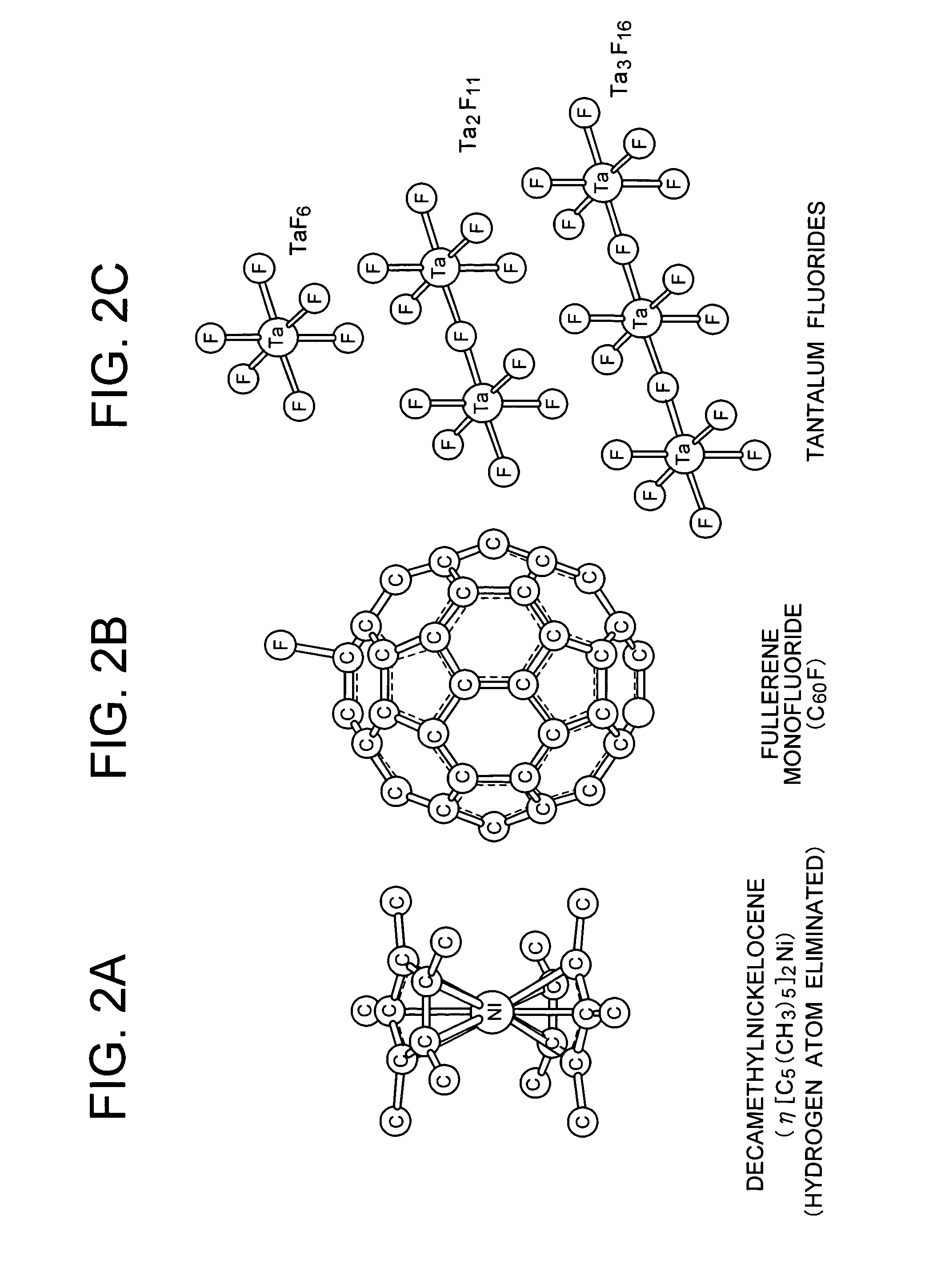
[0053]FIG. 8 is a graph showing the ID-VG characteristic of the carbon nanotube transistor to which decamethylneckelocene positive ions (η[C5(CH3)5]2Ni+) are doped. In FIG. 8, the vertical axis and the horizontal axis represent the same as those of FIG. 7A. In the graph of FIG. 8, “a” shows the state before doping, “b” is the case of doping η[C5(CH3)5]2Ni+ of 1.0×1013 cm−2, “c” is the case of 7.50×1013 cm−2, and “d” is the case of 1.50×1014 cm−2. The source / drain voltage at the time of measurement was 10 mV in all the cases. As in the case of Example 1, the n-type conduction appeared on the plus side of the gate voltage increased in accordance with the increase of the doping concentration, and the p-type conduction on the minus side was suppressed. This indicates that the conduction type of the carbon nanotube channel is converted to the n-type conduction by doping η[C5(CH3)5]2Ni+. It was also observed that the VT value shifted on the minus side in accordance with the increase in th...

example 3

[0054]FIG. 9 is a graph for showing the ID-VG characteristic of the carbon nanotube transistor to which decamethylcobaltocene positive ions (η[C5(CH3)5]2Co+) are doped. In FIG. 9, the vertical axis and the horizontal axis represent the same as those of FIG. 7A. In the graph of FIG. 9, “a” shows the state before doping, “b” is the case of doping η[C5(CH3)5]2Co+ of 2.0×1013 cm−2, “c” is the case of 4.00×1013 cm−2, “d” is the case of 6.00×1013 cm−2, and “e” is the case of 1.00×1014 cm−2. The source / drain voltage at the time of measurement was 10 mV in all the cases. As in the cases of Examples 1 and 2, the n-type conduction appeared on the plus side of the gate voltage increased in accordance with the increase of the doping concentration, and the p-type conduction on the minus side was suppressed. Particularly, in the case of “e” where η[C5(CH3)5]2Co+ of 1.00×1014 cm−2 was doped, most of the p-type conduction disappeared and the carbon nanotube channel was almost perfectly converted to...


PUM

PropertyMeasurementUnit
ionization potentialaaaaaaaaaa
thicknessaaaaaaaaaa
diameteraaaaaaaaaa

Abstract

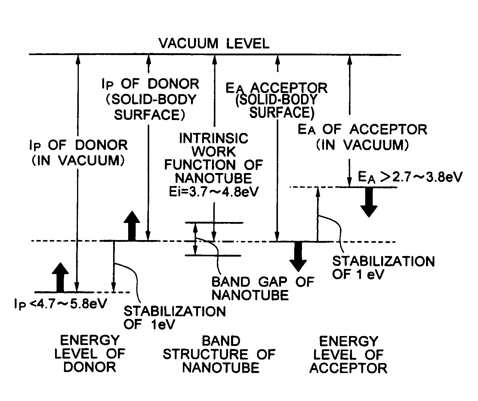
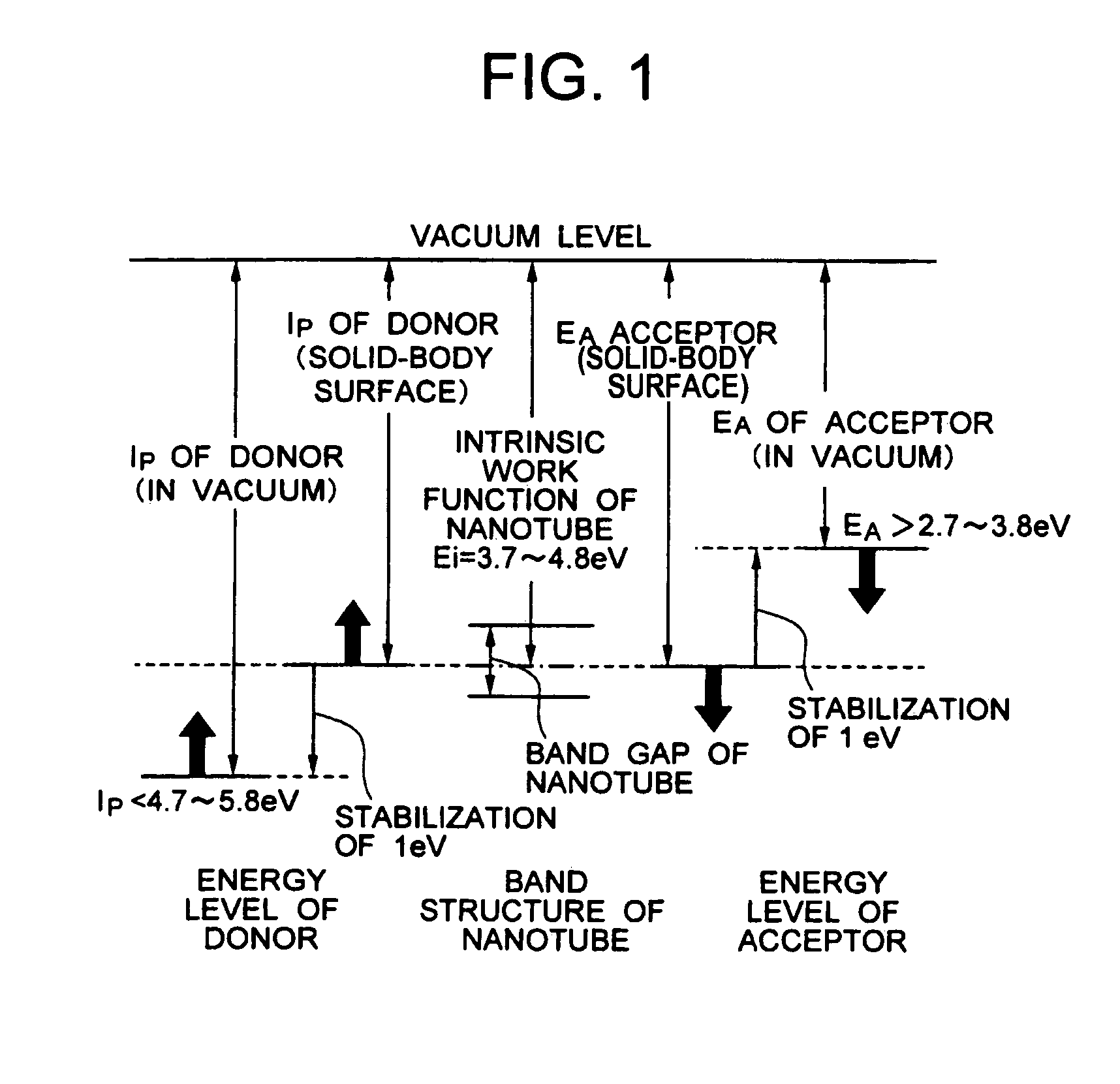
It is to provide a thermodynamically and chemically stable dopant material which can achieve controls of the pn conduction types, carrier density, and threshold value of gate voltage, and a manufacturing method thereof. Further, it is to provide an actually operable semiconductor device such as a transistor with an excellent high-speed operability and high-integration characteristic. Provided is a dopant material obtained by depositing, on a carbon nanotube, a donor with a smaller ionization potential than an intrinsic work function of the carbon nanotube or an acceptor with a larger electron affinity than the intrinsic work function of the carbon nanotube. The ionization potential of the donor in vacuum is desired to be 6.4 eV or less, and the electron affinity of the acceptor in vacuum to be 2.3 eV or more.

Description

BACKGROUND OF THE INVENTION[0001]1. Field of the Invention[0002]The present invention relates to a dopant material using a carbon nanotube, a method for manufacturing the dopant material, and a semiconductor device such as a transistor which is preferable for p-type and n-type conduction semiconductor channels.[0003]2. Description of the Related Art[0004]A carbon nanotube has a tubular graphite structure with a diameter of some nanometers and a length of some hundreds nanometers to some micrometers. Depending on chirality and the diameter, there are metal-type carbon nanotubes and semiconductor-type carbon nanotubes. The semiconductor-type carbon nanotube can be used as a transistor channel. The semiconductor-type carbon nanotube is particularly important as a semiconductor material to be used as post silicon material in terms of device application, since it has more than ten times drift mobility than that of silicon and the structure of the band gap can be controlled by the diamete...

Claims


Application Information

Patent Timeline
Patent Type & Authority Patents(United States)
IPC IPC(8): H01L35/24H10N10/856
CPCB82Y10/00C01B25/42H01L51/002H01L51/0048H10K71/30H10K85/221
Inventor HIURA, HIDEFUMITADA, TETSUYAKANAYAMA, TOSHIHIKO
Owner NAT INST OF ADVANCED IND SCI & TECH
Learn More