CMOS transistors with differential oxygen content high-k dielectrics

a technology of high-k dielectrics and oxygen-containing cmos, which is applied in the direction of transistors, semiconductor devices, electrical apparatus, etc., can solve the problems of limiting the performance of conventional silicon oxide based gate electrodes, unable to fundamentally address the vt shift in high-k dielectrics, and the identification of materials for a dual work function metal gate electrode system has presented some challenges

Inactive Publication Date: 2010-04-13
GLOBALFOUNDRIES INC
View PDF7 Cites 34 Cited by
  • Summary
  • Abstract
  • Description
  • Claims
  • Application Information

AI Technical Summary

Problems solved by technology

High gate leakage current of nitrided silicon dioxide and depletion effect of polysilicon gate electrodes limits the performance of conventional silicon oxide based gate electrodes.
So far, identification of materials for a dual work function metal gate electrode system has presented some challenges.
While metal gate electrodes tend to mitigate the threshold voltage offset effect, no solution has been proposed to fundamentally address the Vt shift in high-k dielectric gates having a polysilicon gate conductor.

Method used


Image

  • CMOS transistors with differential oxygen content high-k dielectrics
  • CMOS transistors with differential oxygen content high-k dielectrics
  • CMOS transistors with differential oxygen content high-k dielectrics

Examples


Embodiment Construction

[0052]As stated above, the present invention relates to semiconductor devices having differential oxygen content high-k dielectrics between p-type MOSFETs and n-type MOSFETs, and methods of manufacturing the same, which are now described in detail with accompanying figures. It is noted that like and corresponding elements are referred to by like reference numerals.

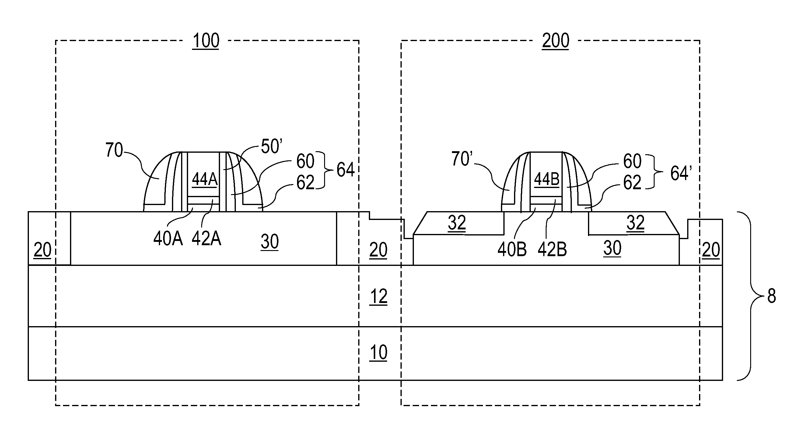
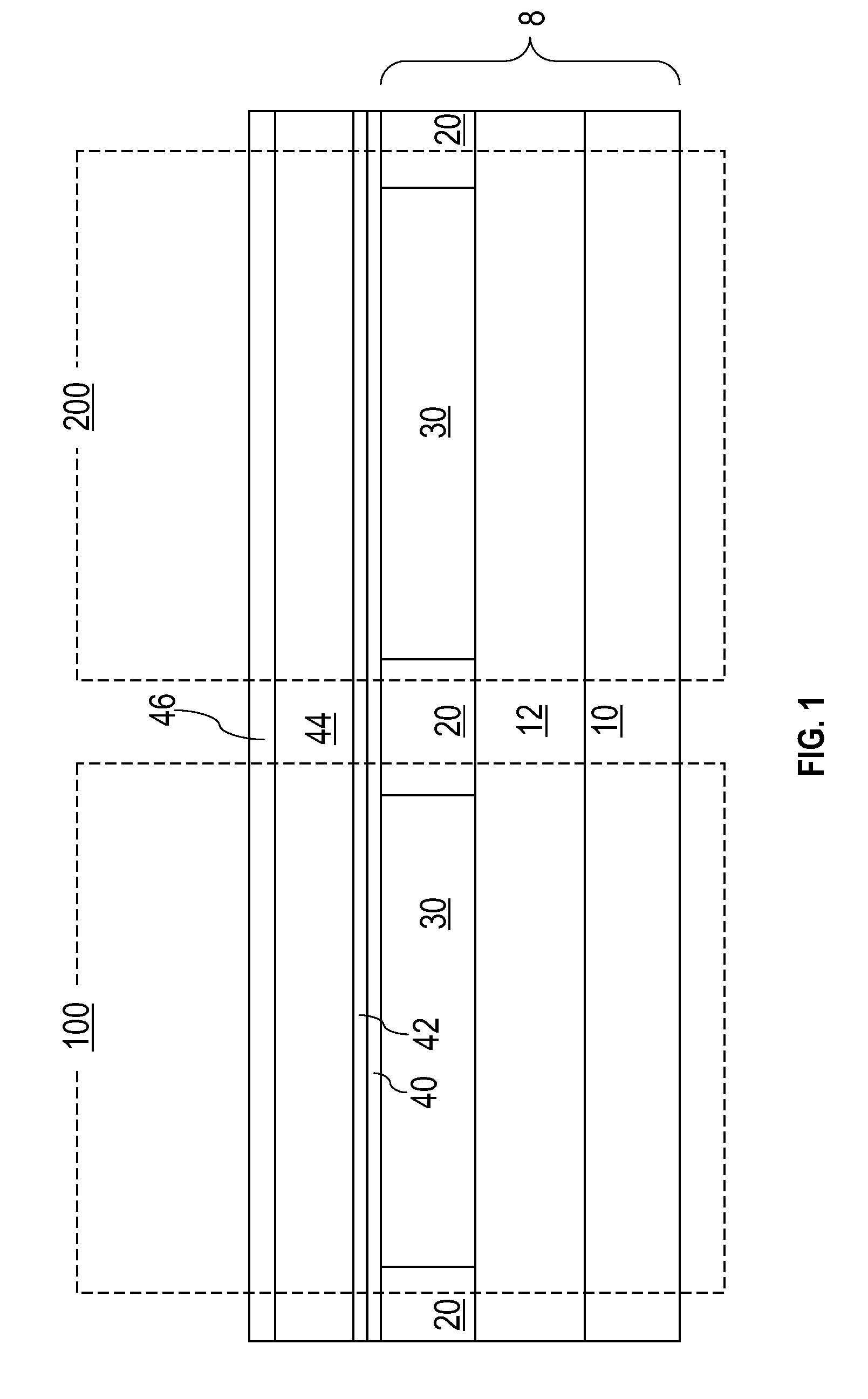
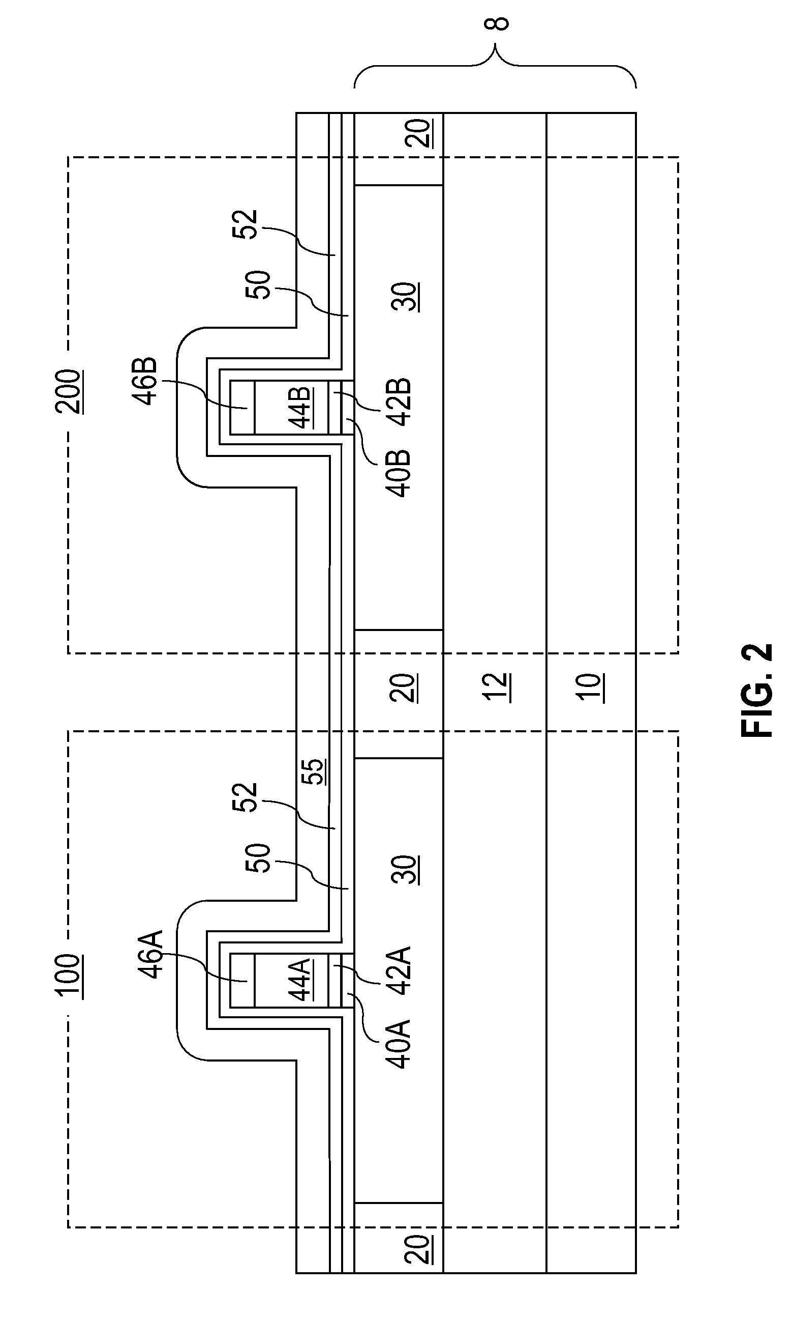
[0053]Referring to FIG. 1, a first exemplary semiconductor structure according to the present invention is shown, which comprises a semiconductor substrate 8 containing a handle substrate 10, a buried dielectric layer 12, and a top semiconductor layer 30. The top semiconductor layer 30 comprises a single crystalline semiconductor material. The semiconductor material may be selected from, but is not limited to, silicon, germanium, silicon-germanium alloy, silicon carbon alloy, silicon-germanium-carbon alloy, gallium arsenide, indium arsenide, indium phosphide, III-V compound semiconductor materials, II-VI compound semicondu...


PUM


Abstract

An NFET containing a first high-k dielectric portion and a PFET containing a second high-k gate dielectric portion are formed on a semiconductor substrate. A gate sidewall nitride is formed on the gate of the NFET, while the sidewalls of the PFET remain free of the gate sidewall nitride. An oxide spacer is formed directly on the sidewalls of a PFET gate stack and on the gate sidewall nitride on the NFET. After high temperature processing, the first and second dielectric portions contain a non-stoichiometric oxygen deficient high-k dielectric material. The semiconductor structure is subjected to an anneal in an oxygen environment, during which oxygen diffuses through the oxide spacer into the second high-k dielectric portion. The PFET comprises a more stoichiometric high-k dielectric material and the NFET comprises a less stoichiometric high-k dielectric material. Threshold voltages of the PFET and the NFET are optimized by the present invention.

Description

FIELD OF THE INVENTION[0001]The present invention generally relates to semiconductor devices, and particularly to semiconductor devices having differential oxygen content high-k dielectrics between p-type MOSFETs and n-type MOSFETs, and methods of manufacturing the same.BACKGROUND OF THE INVENTION[0002]High gate leakage current of nitrided silicon dioxide and depletion effect of polysilicon gate electrodes limits the performance of conventional silicon oxide based gate electrodes. High performance devices for an equivalent oxide thickness (EOT) less than 1 nm require high dielectric constant (high-k) gate dielectrics and metal gate electrodes to limit the gate leakage current and provide high on-currents. Since high-k dielectric materials need to be stable in contact with silicon at a temperature high enough to activate electrical dopants, only a handful of materials are known to be practically useful as a high-k gate dielectric. These include ZrO2, HfO2, other dielectric metal oxid...

Claims


Application Information

Patent Timeline
Patent Type & Authority Patents(United States)
IPC IPC(8): H01L21/8238
CPCH01L21/823857H01L21/823864H01L21/823878H01L29/7848H01L29/6653H01L29/6656H01L29/6659H01L29/66636H01L29/7843H01L21/823814H01L21/84H01L27/1203H01L29/4908H01L29/165
Inventor BU, HUIMINGCARTIER, EDUARD A.DORIS, BRUCE B.KIM, YOUNG-HEELINDER, BARRYNARAYANAN, VIJAYPARUCHURI, VAMSI K.STEEN, MICHELLE L.
Owner GLOBALFOUNDRIES INC
Why Eureka
Try Eureka