FET-based gas sensor

a gas sensor and fet technology, applied in the direction of material thermal analysis material analysis using sonic/ultrasonic/infrasonic waves, etc., can solve the problem of reducing the signal level of the target gas, affecting the sensitivity of the second sensor, and affecting the measurement accuracy

Active Publication Date: 2010-05-04
TDK MICRONAS GMBH
View PDF38 Cites 2 Cited by
  • Summary
  • Abstract
  • Description
  • Claims
  • Application Information

AI Technical Summary

Benefits of technology

[0010]According to one aspect of the invention, a FET gas sensor is configured to measure/detect a target gas in a gas mixture. The FET gas sensor has a gas channel for diffusion of a gas to be measured to a gas-sensitive layer that is in active connection with a field effect trans

Problems solved by technology

Disadvantageously, the aforesaid gas sensors frequently measure reactions from interfering gases (i.e., non-target gases) within the air gap.
As a result, this superposition may distort measurements of the target gas.
In addition, these interfering gases may decrease the signal level of the target gas.
However, similar to the first sensor (i.e., the gas-sensitive material for the target gas), this second sensor may have a limited sensitivity.
However, use of such a filter may prove

Method used


Image

  • FET-based gas sensor
  • FET-based gas sensor
  • FET-based gas sensor

Examples


Embodiment Construction

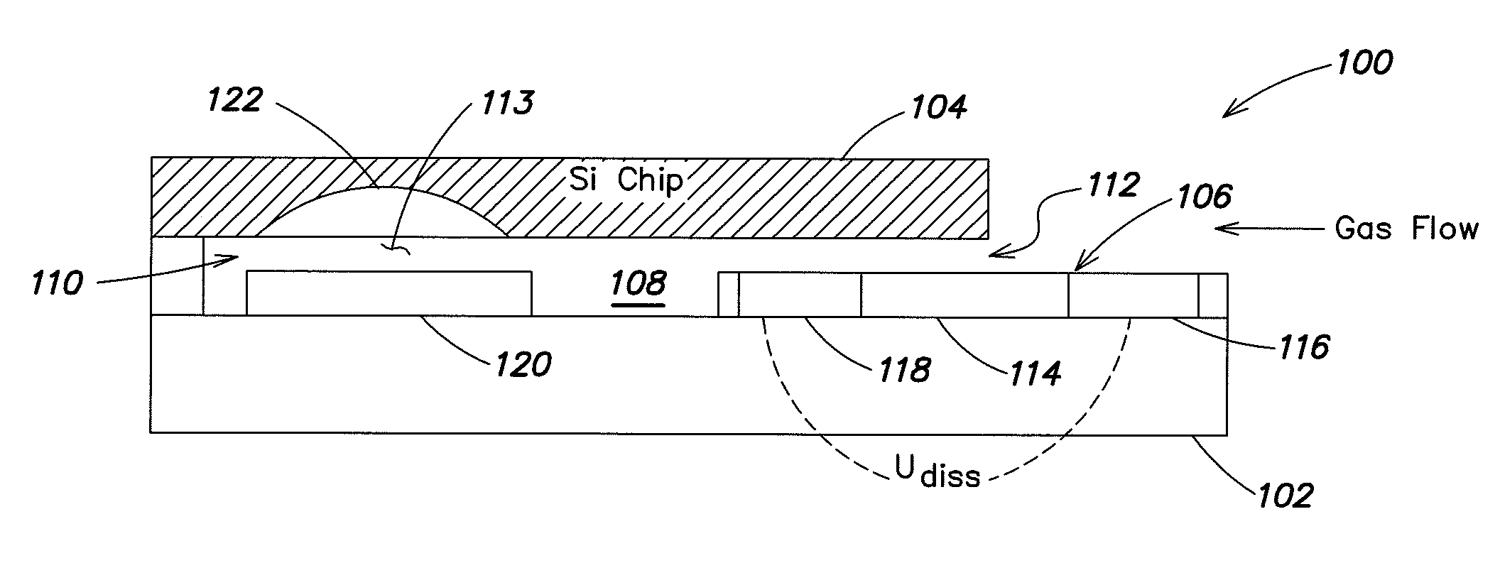
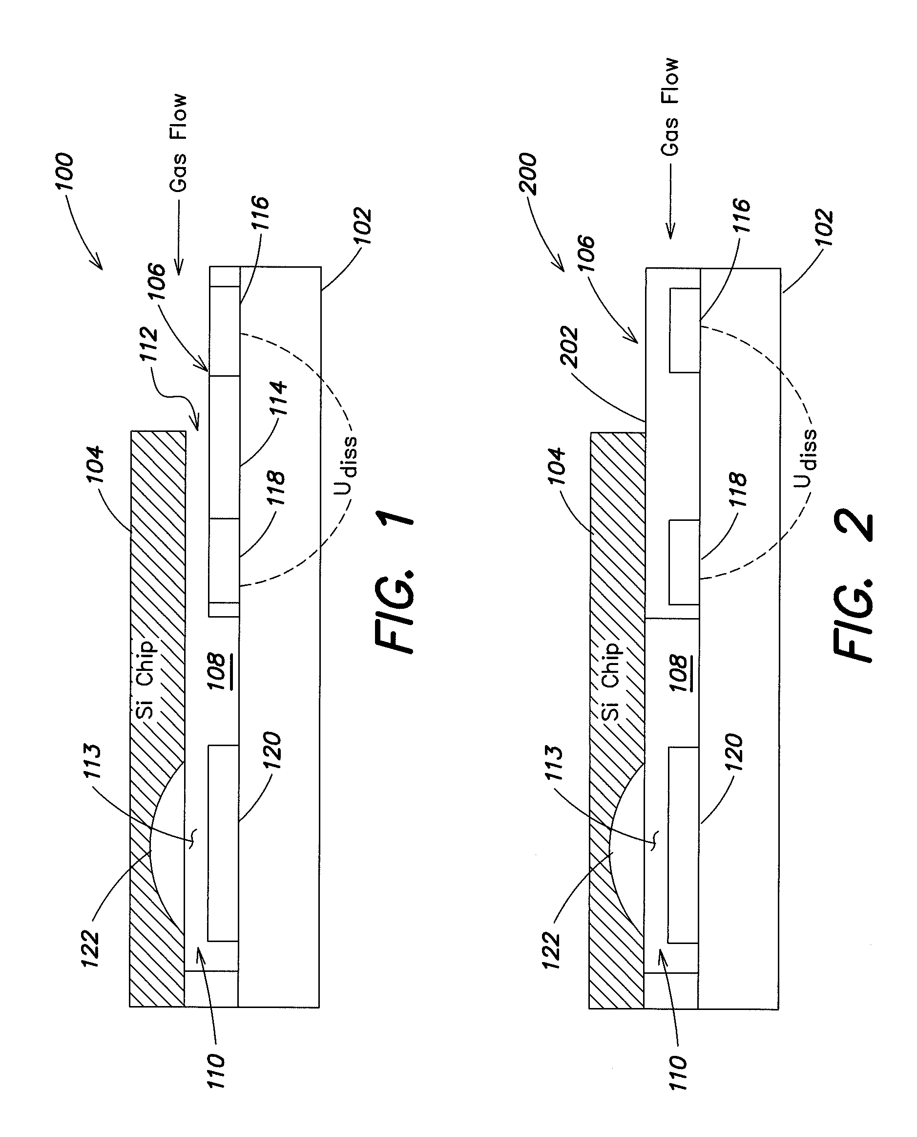
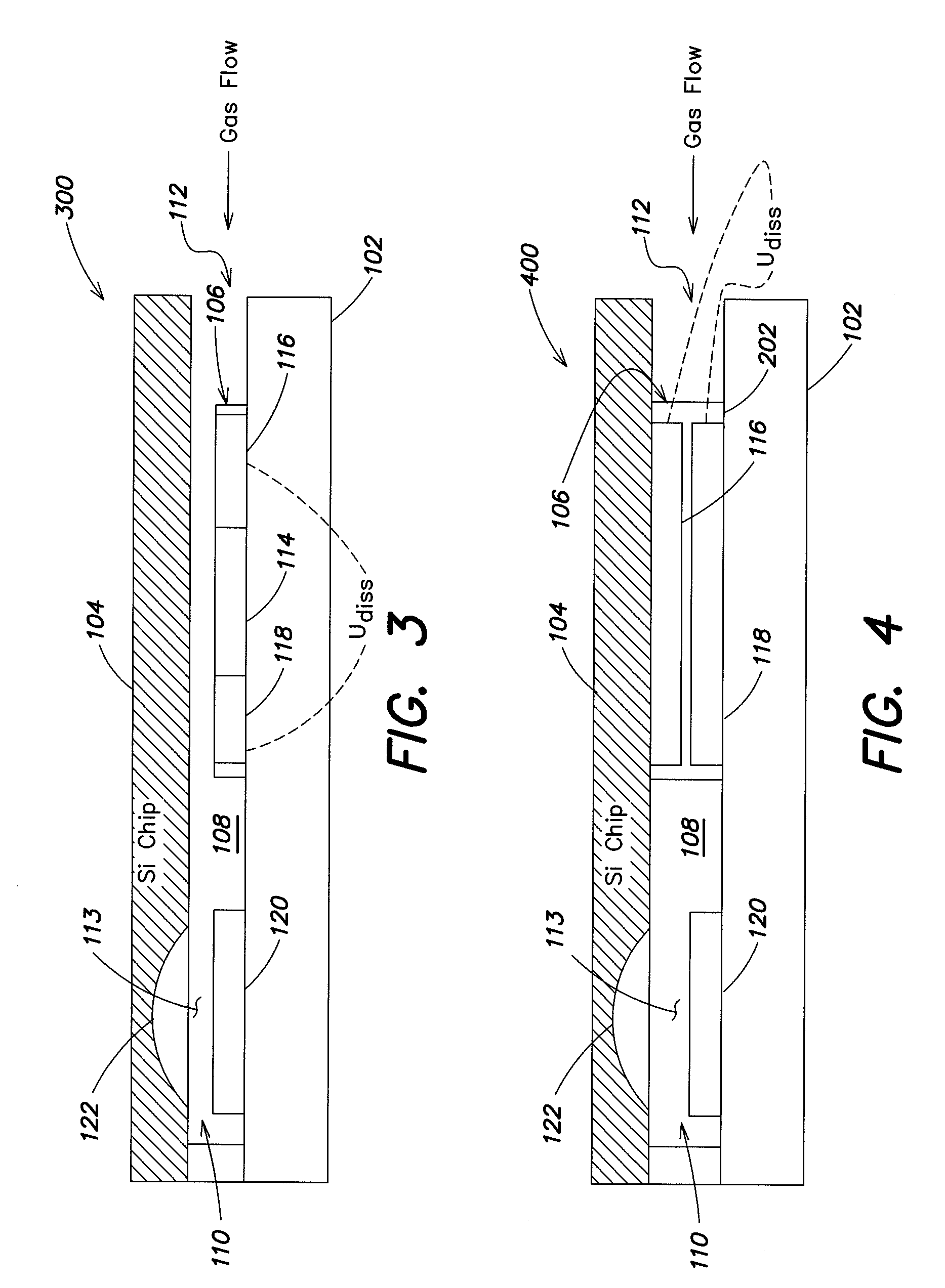
[0026]FIG. 1 illustrates one embodiment of an FET gas sensor system 100. The sensor 100 includes a carrier substrate 102, a chip 104 (e.g., a silicon chip), an electrochemical element / structure 106, a gas channel 108 (also referred to as a “gas diffusion channel”), and a detection area 110.

[0027]The carrier substrate 102 is constructed from any desired nonconductive material that allows, for example, only the preparation of the layers disposed on it. Suitable materials include, but are not limited to, ceramics (e.g., Al2O3, AlN, or Si3N4), glasses, or polymeric materials (e.g., conventional PCB materials like FR4 or the like).

[0028]The gas channel 108 includes an air inlet 112. The air inlet 112 is defined between the silicon chip 104 and the electrochemical element 106 such that entry of gas (or a gas mixture) and its diffusion to a sensor area / gas gap 113 (i.e., the region between the sensitive layer 120 and the transistor 122) is sharply limited. That is, the air inlet 112 thus t...


PUM


Abstract

An operating method is disclosed for the selective detection of a target gas in a gas mixture to be measured by a field effect transistor with a gas-sensitive layer disposed on a carrier substrate, wherein the gas mixture to be measured is prepared by an electrochemical element such that the measured gas mixture includes minimal amounts of interfering gases that interfere with the measurement of the target gas, and/or at least one target gas is activated such that it is detected by the gas-sensitive layer.

Description

PRIORITY INFORMATION[0001]This patent application claims priority from International patent application PCT / EP2005 / 004278 filed Apr. 22, 2005 and German patent application 10 2004 019 641.9 filed Apr. 22, 2004, which are hereby incorporated by reference in their entirety.BACKGROUND INFORMATION[0002]Typically, a field effect transistor (“FET”) gas sensor measures a change in a work function between a gas-sensitive material and a reference material. FIG. 6 is a schematic illustration of such a FET gas sensor 10. A gateless transistor 12 is capacitively coupled, through an air gap 14, to a gas-sensitive layer 16. The air gap 14 is configured as a gas inlet a few micrometers (μm) wide. The gas-sensitive layer 16 is adapted such that its surface potential changes upon contact with a gas within the air gap 14, and thus controls the transistor 12. The working temperatures of such a sensor are between ambient temperature and 150° C.[0003]FIG. 7 is a diagrammatic illustration of a typical su...

Claims


Application Information

Patent Timeline
IPC IPC(8): G01N33/00B01L5/00G01N27/00G01N27/407G01N27/414
CPCG01N27/4143G01N33/0013
Inventor FLEISCHER, MAXIMILIANMEIXNER, HANSSIMON, ELFRIEDELAMPE, UWEPOHLE, ROLAND
Owner TDK MICRONAS GMBH
Why Eureka
Try Eureka