Data storage device and method

a data storage and data technology, applied in the field of data storage, can solve the problems of inability to use in high vibration or high shock environments, inability to miniaturize well, and inability to meet the needs of high-speed data storage, etc., to achieve easy scalability, high storage density, and simplified scalability in the vertical dimension

Inactive Publication Date: 2010-05-04
INGENIA HLDG LTD
View PDF13 Cites 17 Cited by
  • Summary
  • Abstract
  • Description
  • Claims
  • Application Information

AI Technical Summary

Benefits of technology

[0031]The above approach has several advantages. First, data can be clocked through the device with a global externally applied field, i.e. the clocking field. No addressing of individual pinning sites, i.e. nanowire crosses, or groups of pinning sites is needed. This is because the novel clocking mechanism provided by the combination of nanowire crosses and clocking field is not sensitive to the charge state of the domain wall, i.e. whether the domain wall is a head-to-head domain wall or a tail-to-tail domain wall. The same field can thus be applied to all pinning sites to move the data incrementally through the nanowire pinning sites. Second, the structure is readily scalable in three dimensions in that multiple layers of nanowire networks can be arranged on top of each other, thus providing a very high storage density. This scalability in the vertical dimension is simplified by the fact that data can be clocked through the device with a global externally applied field. Third, the novel approach of encoding the data in the chirality of the domain walls allows for relatively dense data storage in comparison with previously proposed magnetic nanowire serial memories which use properties of the domains themselves, such as domain length, to encode the data.
[0032]A further magnetic field source may be provided which is operable to generate an operating field aligned with the data-carrying nanowires, which serves to assist movement of the data-carrying domain walls along the data-carrying nanowires between cross junctions.

Problems solved by technology

Spinning disk systems suffer from unreliability of the mechanical components (such as the disk bearings), cannot be miniaturized well, and cannot be used in high vibration or high shock environments.
Any contamination of the surface through dust particles or other foreign bodies or warping or other non-flatness of the surface can result in failure to read / write or catastrophic failure of the device by crashing of the head.
Moreover, access times are of a mechanical time scale and in a PC severely limit the microprocessor's performance.
It is estimated that in a PC up to one third of the instruction cycles of a microprocessor can be wasted by waiting for the hard disk.
However, with current technology semiconductor memory is still too costly to displace hard drives.
Moreover, such memories suffer from problems associated with limited write endurance and write latency.
In particular, flash memory has a life cycle of up to approximately 1000 write operations before degradation of reliability and performance occurs.
Also, the write latency for flash memory is high due to the need to charge a large capacitance for the data storage.
Both disk drives and flash memory have important limitations in the density of information that they can store by today's state-of-the-art lithography.
Storage densities of both of these technologies will thus be unable to make order of magnitude leaps without a sudden (and unexpected) change in lithography performance.
This miniaturization can only be achieved with very high density memory.
However, the only approach to 3-dimensional solid state memory available at the moment is simply to layer devices on top of each other, each layer requiring electrical connection.
However, as well as being a breakthrough, using this spin-polarization effect is at the same time a serious limitation for any device based on this principle.
This is because the current-induced propagation along the nanowire of the head-to-head and tail-to-tail domain walls needs to be under complete control, since if adjacent head-to-head and tail-to-tail domain walls do not propagate at near equal speed, they will come together and annihilate, thereby corrupting the data encoded by the domains.
To achieve the necessary control of the propagation speed in such devices will become increasingly challenging from a fabrication point of view as such devices is scaled up from a prototype stage to a production device.
Consequently, in our view at least, it is by no means certain that this type of device can successfully be developed into a commercial product.
This requirement places a limitation on the maximum density of information that can be coded.

Method used


Image

  • Data storage device and method
  • Data storage device and method
  • Data storage device and method

Examples


Embodiment Construction

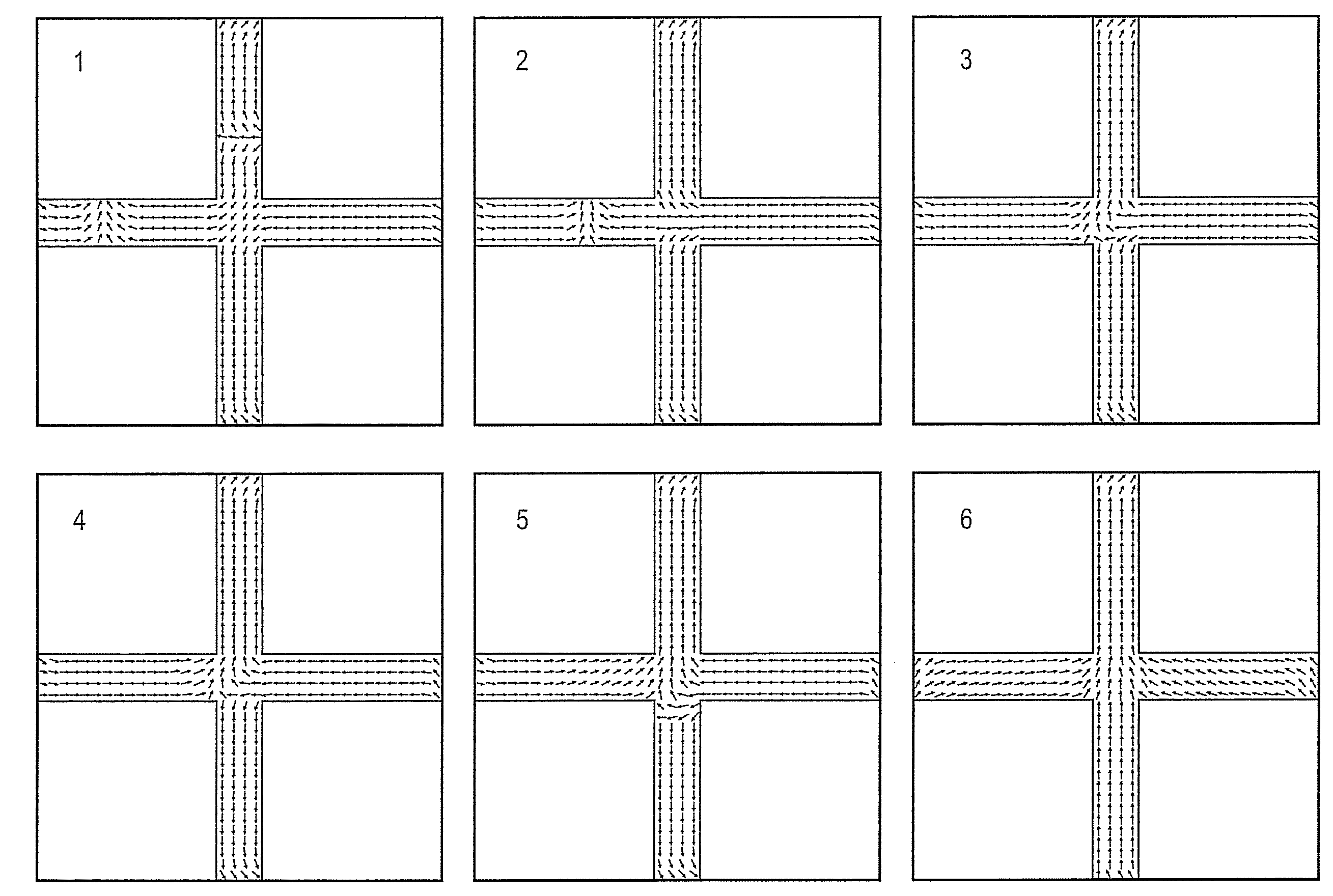
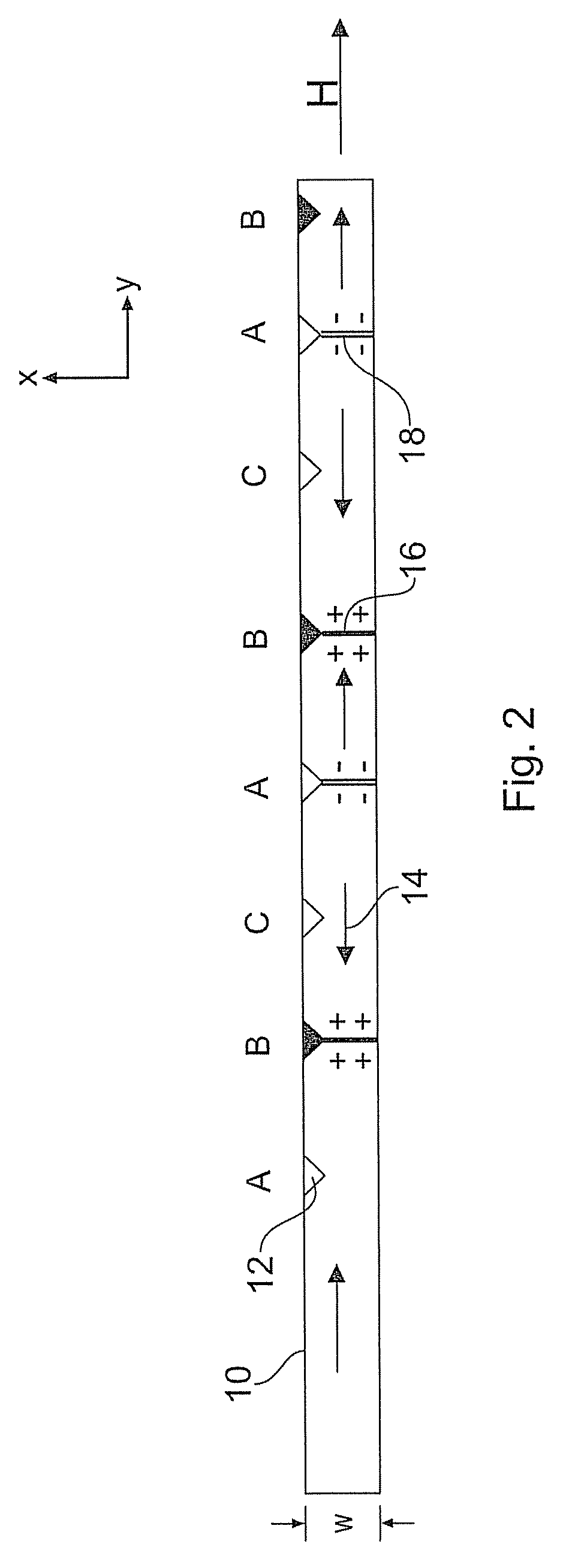
[0083]FIG. 3A is a schematic plan view representation of a magnetic nanowire structure embodying to the invention. The following convention is adopted throughout for the axes. The z axis is the vertical axis, the x and y axes are horizontal. The basic structure is a cross formed by a first nanowire 100 extending in the x direction and a second nanowire 110 extending in the y direction which cross each other at a junction 115.

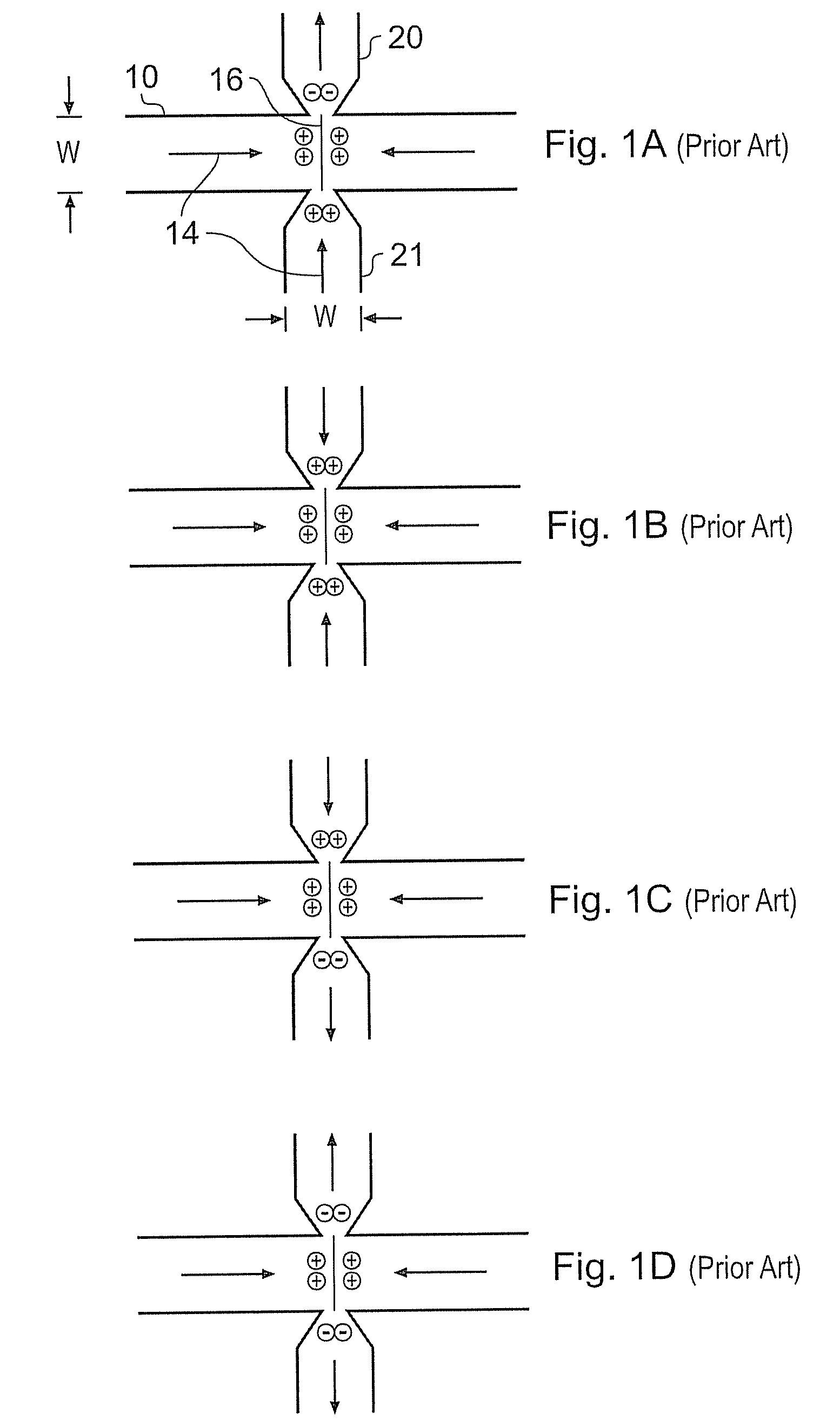
[0084]The magnetic domains 114 hosted in the nanowires 100 and 110 are illustrated with arrows indicating the magnetic moment in the conventional way. Each domain is bounded by a domain wall 112. As is understood in the art, the nanowire domain walls fall into two types, head-to-head domain walls, such as the illustrated domain wall 112 and tail-to-tail domain walls, the meaning of which will be self-explanatory. Head-to-head domain walls carry positive magnetostatic charge and tail-to-tail domain walls carry negative magnetostatic charge. The positive and negat...


PUM


Abstract

A serial magnetic mass storage device and associated data storage method is provided based on magnetic nanowires that support single magnetic domains separated by domain walls. Each data-storing nanowire has a plurality of crossing nanowires along its length, forming cross junctions that constitute domain wall pinning sites. Data is fed through each data-storing nanowire by moving the magnetic domains under the action of a field that alternates between alignment and anti-alignment with the crossing nanowires. The data is encoded in the chirality of the domain walls, with up and down chirality transverse domain walls being used to encode 0's and 1's. Data is clocked into each nanowire with suitable nucleation generators capable of nucleating domains with domain walls of pre-defined chirality. Data is clocked out of each nanowire with suitable magnetic field sensors that sense the chirality.

Description

FIELD OF THE INVENTION[0001]The present invention relates to data storage, more especially but not exclusively to mass storage memory devices capable of storing GBytes of data, and of storing data at high densities.[0002]Hard drives with magnetic disks are the dominant technology for mass data storage and retrieval in personal computers (PCs). With current technology hard disk drives have storage capacities of up to around 100-200 GBytes, although smaller capacity miniature units are used in some devices, such as portable music players, video players and other portably multimedia devices which typically have drive capacities in the range 30-40 GBytes, or even smaller devices for digital cameras of sub-10 GBytes. The basic structure of a hard drive can trace its heritage back to a 19th century gramophone, in that it is fundamentally a mechanical device based on a spinning disk with a pivotally mounted arm that can be positioned over the disk to read (and write) data stored on the dis...

Claims


Application Information

Patent Timeline
Patent Type & Authority Patents(United States)
IPC IPC(8): G11C11/14
CPCG11C19/0808Y10S977/933
Inventor COWBURN, RUSSELL PAULPETIT, DOROTHEEREAD, DAN
Owner INGENIA HLDG LTD
Why Eureka
Try Eureka