Method and apparatus for backside polymer reduction in dry-etch process

a technology of dry etching and backside polymer, which is applied in the direction of mechanical equipment, chucks, manufacturing tools, etc., can solve the problems of destroying an entire semiconductor device, contaminating the chamber, and common buildup, so as to prevent or reduce the formation of polymeric films, reduce contamination, and reduce the effect of contamination

Inactive Publication Date: 2010-05-11
TAIWAN SEMICON MFG CO LTD
View PDF27 Cites 18 Cited by
  • Summary
  • Abstract
  • Description
  • Claims
  • Application Information

AI Technical Summary

Benefits of technology

[0005]To achieve these and other objects and in view of its purposes, the present invention addresses the shortcomings of conventional plasma etching process technologies and provides a plasma etching operation that reduces contamination by preventing or reducing the formation of polymeric films on the substrates being etched.

Problems solved by technology

Semiconductor devices are especially sensitive to particle contamination and the presence of one very small particle can destroy an entire semiconductor device.
The polymers can adhere to various surfaces within the etch chamber and become dislodged, contaminating the chamber.
One particularly prevalent and problematic location where polymer buildup is common, is the backside of a semiconductor substrate being etched, particularly at the peripheral edge of the substrate.
When a polymer film is formed on the peripheral edge of a semiconductor substrate, any jarring of the substrate or movement of the substrate which causes the edge of the substrate to contact another surface, typically causes the polymeric film to delaminate and flake.
This generates particles that may fall immediately on the top, device side of the substrate or at least contaminate the chamber in which the substrate is located, which may ultimately result in device contamination and failure.
Such a thick polymer film can result in the generation of considerable particle contamination which can destroy devices and lower yield.

Method used


Image

  • Method and apparatus for backside polymer reduction in dry-etch process
  • Method and apparatus for backside polymer reduction in dry-etch process
  • Method and apparatus for backside polymer reduction in dry-etch process

Examples


Embodiment Construction

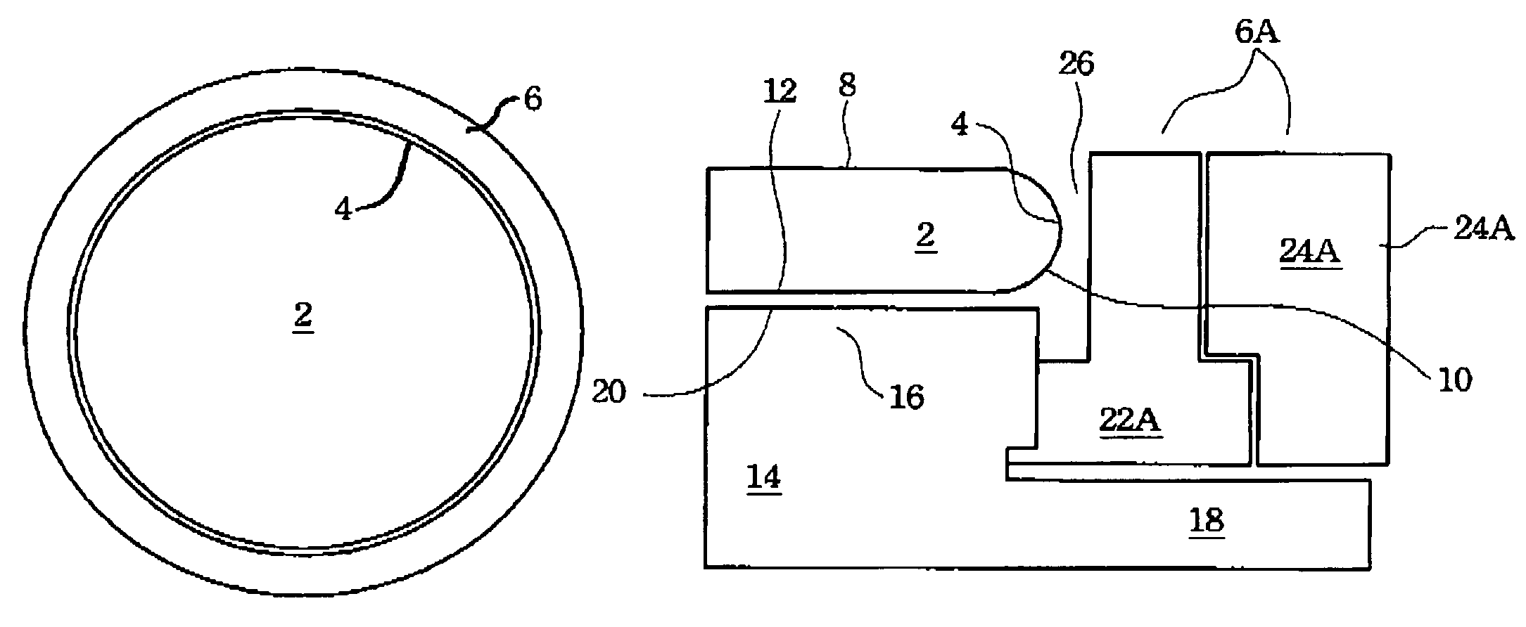
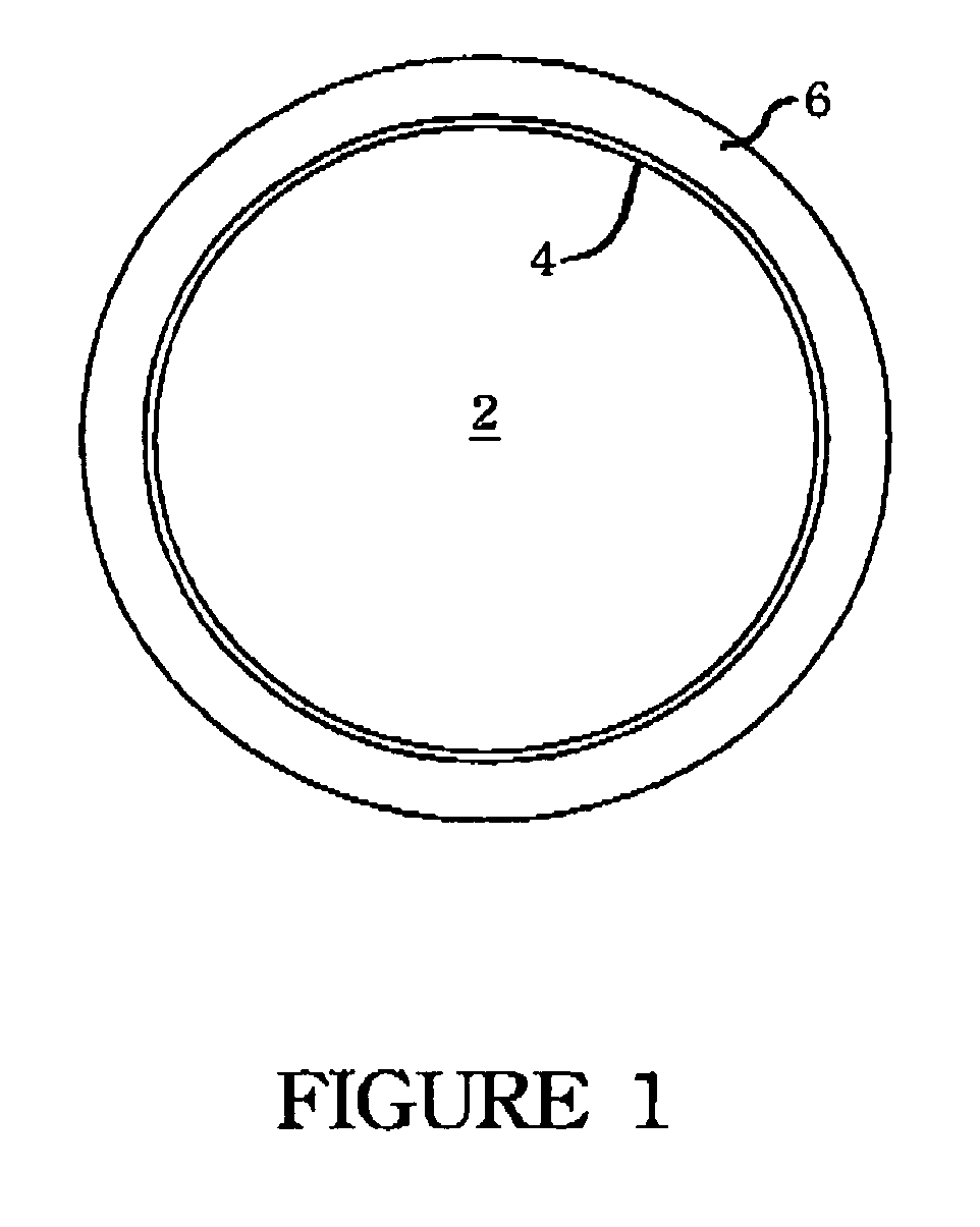
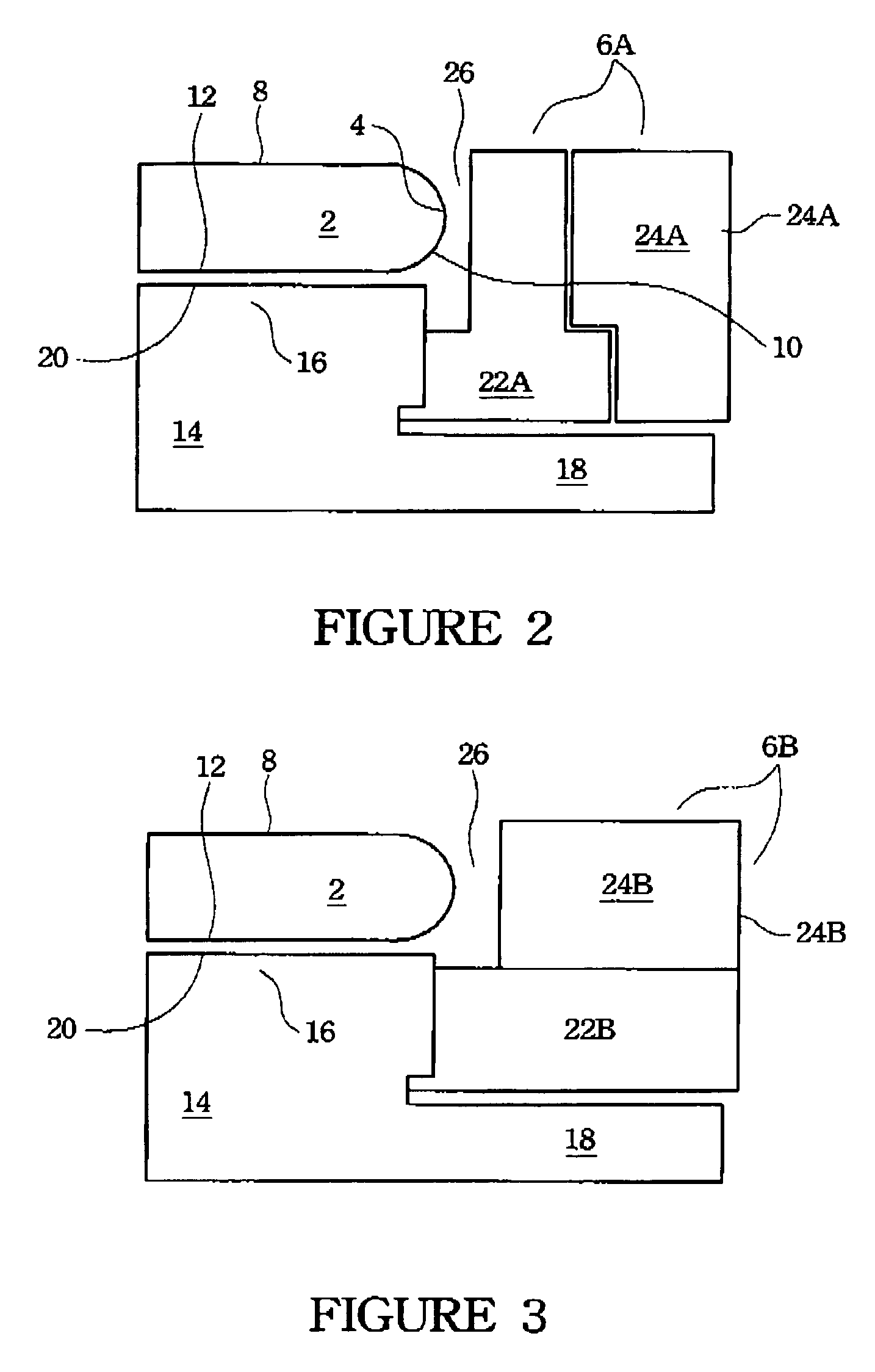
[0021]The present invention is directed to a method and apparatus for eliminating or preventing the formation of polymer film on the backside of a substrate, also known as a wafer, during dry / plasma etching operations used to pattern films or other features formed on the front side of the substrate. The present invention applies to various substrate sizes and various substrate materials upon which semiconductor devices are formed. Silicon and gallium arsenide are examples of semiconductor substrate materials commonly used in today's semiconductor manufacturing industry. The method and apparatus of the present invention applies to various plasma etching tools manufactured by various equipment manufacturers. The method and apparatus of the present invention may be used in various types of dry etching operations used to etch various films at various stages in the semiconductor device manufacturing processing sequence. Reactive ion etching, RIE, is such an exemplary dry etching operatio...


PUM

PropertyMeasurementUnit
thicknessaaaaaaaaaa
thicknessaaaaaaaaaa
pressureaaaaaaaaaa

Abstract

A method for preventing the formation of contaminating polymeric films on the backsides of semiconductor substrates includes providing an oxygen-impregnated focus ring and / or an oxygen-impregnated chuck that releases oxygen during etching operations. The method further provides delivering oxygen gas to the substrate by mixing oxygen in the cooling gas mixture, maintaining the focus ring at a temperature no greater than the substrate temperature during etching and cleaning the substrate using a two step plasma cleaning sequence that includes suspending the substrate above the chuck.

Description

FIELD OF THE INVENTION[0001]The present invention relates, most generally, to semiconductor devices and methods for forming the same. More particularly, the present invention relates to a method and apparatus for backside polymer reduction in dry etching operations.BACKGROUND[0002]Yield enhancement is a goal in virtually all manufacturing processes including manufacturing processes used in the semiconductor manufacturing industry. In the semiconductor manufacturing industry where device feature sizes can be in the nanometer range, there is a close correlation between device yield and contamination levels. Semiconductor devices are especially sensitive to particle contamination and the presence of one very small particle can destroy an entire semiconductor device. It is therefore desirable to reduce particle contamination in each of the multitude of manufacturing processes used to form a semiconductor device.[0003]Dry etching processes, also referred to as plasma etching processes, a...

Claims


Application Information

Patent Timeline
Patent Type & Authority Patents(United States)
IPC IPC(8): C23F1/00B23B31/28H01L21/683H01J37/32H01L21/00H01L21/302H01L21/306H01L21/3065H01L21/311H01L21/461H01L21/687
CPCH01J37/3244H01J37/32642H01L21/02046H01L21/31116H01L21/68735H01L21/67069Y10T279/23Y10S156/914Y10S156/915
Inventor CHEN, HUANG-MINGCHOU, CHUN-LICHEN, CHAO-CHENGTAO, HUN-JAN
Owner TAIWAN SEMICON MFG CO LTD
Why Eureka
Try Eureka