
Photoactive nanocomposite and method for the production thereof

a technology of photoactive nanocomposite and nanocomposite, which is applied in the field of photoactive nanocomposite, can solve the problems of poor charge mobility, not very stable, and limited usefulness of these systems

Inactive Publication Date: 2010-05-11
COMMISSARIAT A LENERGIE ATOMIQUE ET AUX ENERGIES ALTERNATIVES +2
View PDF6 Cites 55 Cited by
  • Summary
  • Abstract
  • Description
  • Claims
  • Application Information

AI Technical Summary

Benefits of technology

[0041]or the nanowires formed on the ITO layer, and making the first electrod...

Problems solved by technology

However, they are not very stable (ageing).
The usefulness of these systems is limited in particular by the flow of charge in organic materials.
Indeed, in most organic conductors, charge mobility is poor (less than 10−4 cm2Vs−1) because of the presence of charge traps such as oxygen.
Furthermore, they are not very stable in air.

Method used


Image

  • Photoactive nanocomposite and method for the production thereof
  • Photoactive nanocomposite and method for the production thereof
  • Photoactive nanocomposite and method for the production thereof

Examples


first embodiment

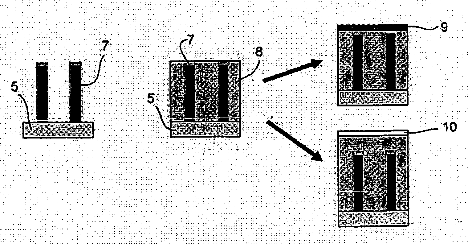
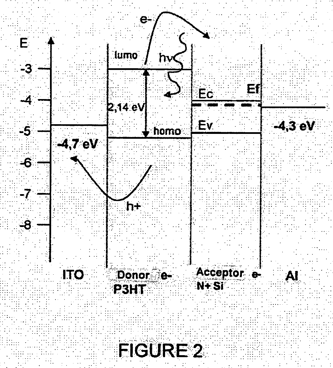
[0054]In a first embodiment, the data shown in FIG. 2 are used, the active layer 3 is placed between a tin doped indium oxide (ITO) electrode 2 and an aluminum electrode 9.

second embodiment

[0055]In a second embodiment, the active layer 3 is placed between a tin doped indium oxide (ITO) electrode 2 and a gold electrode 10, FIG. 3 depicts the diagram of groups of these materials.

[0056]FIGS. 2 and 3 respectively show, in each case, the Fermi level of the materials making the nanowires 7, the organic compound 8 and the materials constituting the electrodes 9 and 10.

[0057]To optimise output of the cell, the materials used must be optimised. The following parameters can be adjusted:

[0058]1°—Doping of the nanowires: knowing the HOMO (High Occupied Molecular Orbital) and LUMO (Low Unoccupied Molecular Orbital) levels of Regioregular P3HT, the Fermi level of the nanowires 7 is altered by determining the dopant concentration for the silicon. The silicon nanowires 7 must be doped p-type electron acceptors (since the P3HT is an n-type electron donor).

[0059]2°—The nanowire diameter: it is known that the energy band gap varies as a function of nanowire 7 diameter. For diameters of ...


PUM

PropertyMeasurementUnit
Nanoscale particle sizeaaaaaaaaaa
Electrical conductoraaaaaaaaaa
Transparencyaaaaaaaaaa

Abstract

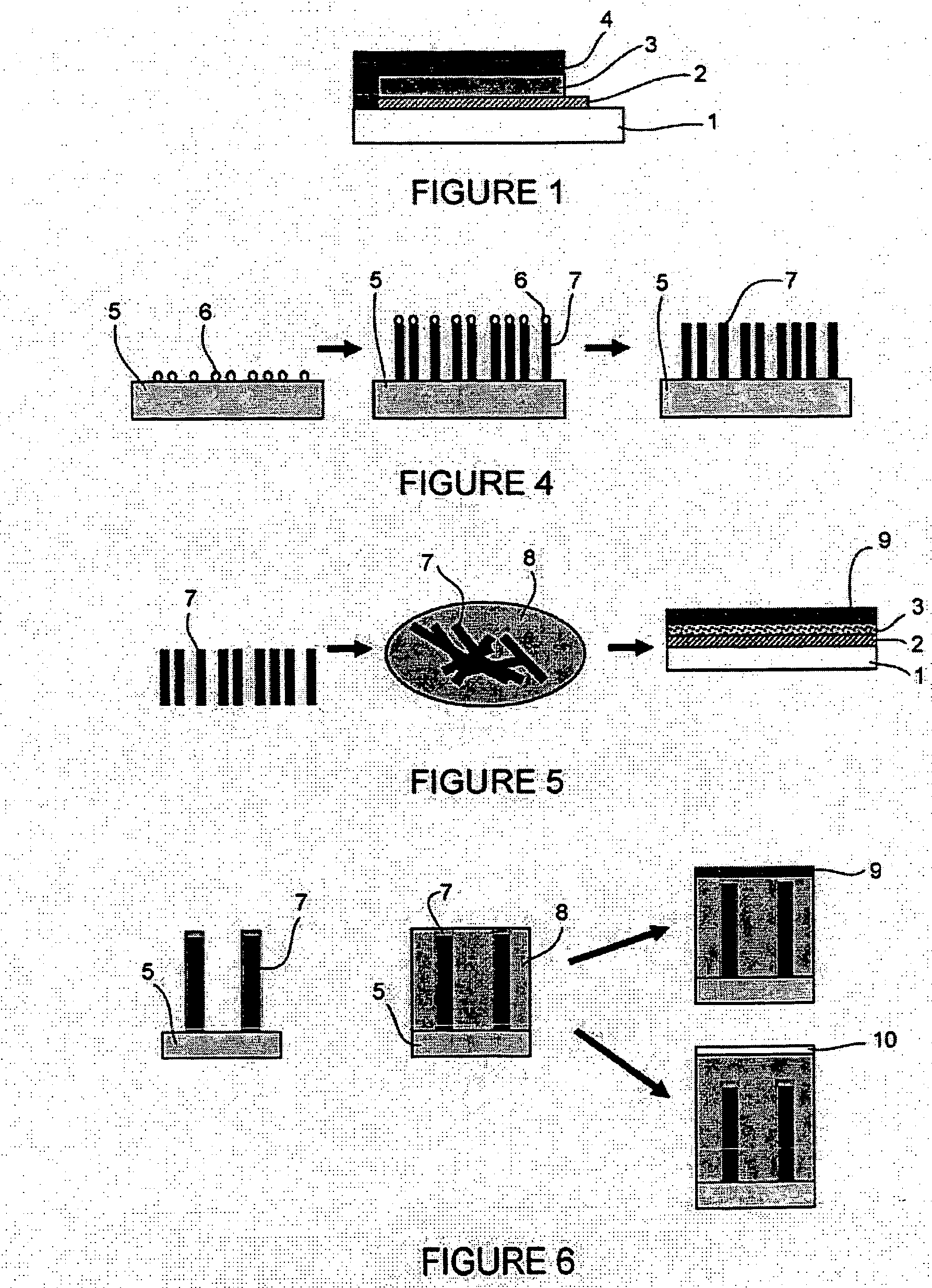
The invention concerns a photoactive nanocomposite (3) comprising at least one donor-acceptor couple of semiconductor elements. One of the elements is made of doped nanowires (7) with sp3 structure, and the other of the elements is an organic compound (8). The elements are supported by a device substrate (1). The invention also concerns a production method. According to a first embodiment, after their growth, the nanowires (7) are retrieved, functionalised and solubilised in the organic component (8). The mixture is deposited by coating on a device substrate. According to a second embodiment, the nanowires (7) are formed on a growth substrate (5) which is also the device substrate. The organic component (8) is combined with the nanowires (7) so as to form an active layer (3). Such a photoactive nanocomposite (3) allows production of a photovoltaic cell.

Description

BACKGROUND OF THE INVENTION[0001]1. Fields of the Invention[0002]The present invention concerns a photoactive nanocomposite capable of being used in a solar cell to induce the photovoltaic effect, in a light emitter or in a photodetector.[0003]2. Description of the Related Art[0004]This type of photoactive component conventionally comprises a donor-acceptor couple of semiconductor elements. It is known that to see a charge transfer between donor and acceptor, the respective energy levels of the former and the latter must be compatible.[0005]Photovoltaic devices based on amorphous or thin film microcrystalline silicon are familiar. These devices deliver a significant output of 6 to 10%. However, they are not very stable (ageing). Materials of the interpenetrating network type—conjugated polymer and fullerene or its derivatives—are also familiar. The usefulness of these systems is limited in particular by the flow of charge in organic materials. Indeed, in most organic conductors, cha...

Claims


Application Information

Patent Timeline
IPC IPC(8): H01L51/40H01L51/30
CPCB82Y10/00B82Y30/00H01L51/4213H01L51/4266H01L51/0048H01L51/002H01L51/0036Y02E10/549H01L2251/308H10K71/30H10K85/113H10K85/221H10K30/10H10K30/352H10K2102/103H10K30/50
Inventor FIRON, MURIELDREVILLON, BERNARDFONTCUBERTA I MORRAL, ANNAPALACIN, SERGEROCA I CABARROCAS, PERE
Owner COMMISSARIAT A LENERGIE ATOMIQUE ET AUX ENERGIES ALTERNATIVES
Learn More