
Manufacturing method of printed circuit board

a manufacturing method and printed circuit board technology, applied in the direction of printed circuit aspects, printed element electric connection formation, conductive pattern formation, etc., can solve the problems of difficult to reliably perform etching, disadvantage of fine line formation, and thickening of the entire metal layer, so as to reduce the depth of the via hole on the land, improve the effect of thickness and finer material

Inactive Publication Date: 2010-06-01
GLOBALFOUNDRIES U S INC
View PDF17 Cites 16 Cited by
  • Summary
  • Abstract
  • Description
  • Claims
  • Application Information

AI Technical Summary

Benefits of technology

The present invention provides a method and printed circuit board that can adjust the aspect ratio of via holes and form fine lines. The method includes preparing an insulating substrate with metal foil on both sides, selectively forming a plating layer for forming a land, adjusting the thickness of the plating layer, and forming the metal foil into a line. The printed circuit board includes lines of metal foil and lands formed of a stack of metal foil and plating layer, with a via hole formed on the lands. The method and printed circuit board enable finer lines and reduced aspect ratio of via holes.

Problems solved by technology

If plating is performed on the metal conductor layer in an area where lines will be formed, the entire metal layer becomes thick and it is difficult to reliably perform etching so that the lines have a predetermined line and a line spacing.
This is a disadvantage to forming of fine lines.
If the insulating layer is a prepreg containing glass cloth, the thickness of the insulating layer is limited by the thickness of the glass cloth and cannot be reduced.
If the diameter of the via holes is reduced, the aspect ratio of the via holes becomes higher and the plating liquid cannot flow smoothly to the bottom of each via hole.
As a result, the plating layer at the bottoms of the via holes is made nonuniform in thickness and there is a possibility of occurrence of a crack in the plating layer at the reflow temperature at the time of mounting or in a thermal cycle test and, hence, a possibility of failure to establish interlayer connection.
This is a disadvantage to forming of fine lines.
As described above, it is difficult to reliably perform plating on via holes and to form fine lines.
Also, at the time of etching for forming the lines, failure to completely performing etching may occur due to variation in thickness of the plating layer and there is a possibility of short circuit between the lines in some place.
However, there is a possibility of the bond strength of the plating layer to the insulating substrate becoming lower than that of the metal foil, i.e., failure to obtain the desired metal bond strength.
There is a risk of the plating layer being separated from the insulating substrate when the completed printed circuit board is subject to various tests including a thermal shock test.
If the plating layer is separated, the printed circuit board cannot be used as the product.
In a case where plating processing is performed directly on an insulating member, there is a possibility of a catalyst such as palladium used in plating processing remaining as a residue to cause insulation degradation.
If the catalyst remains as a residue between conductors, there is a risk of occurrence of failure phenomenon such as short circuit between pads when gold plating processing is performed and insulation degradation caused by an electrocorrosion test.
Therefore, it is difficult to form fine lines even if interlayer connection can be established with reliability.
However, formed lines are also plated, so that it is difficult to form fine lines.
The difficulty in forming fine lines is further increased thereby.

Method used


Image

  • Manufacturing method of printed circuit board
  • Manufacturing method of printed circuit board
  • Manufacturing method of printed circuit board

Examples


Embodiment Construction

[0043]A printed circuit board manufacturing method and a printed circuit board manufactured by the manufacturing method will be described with reference to the drawings.

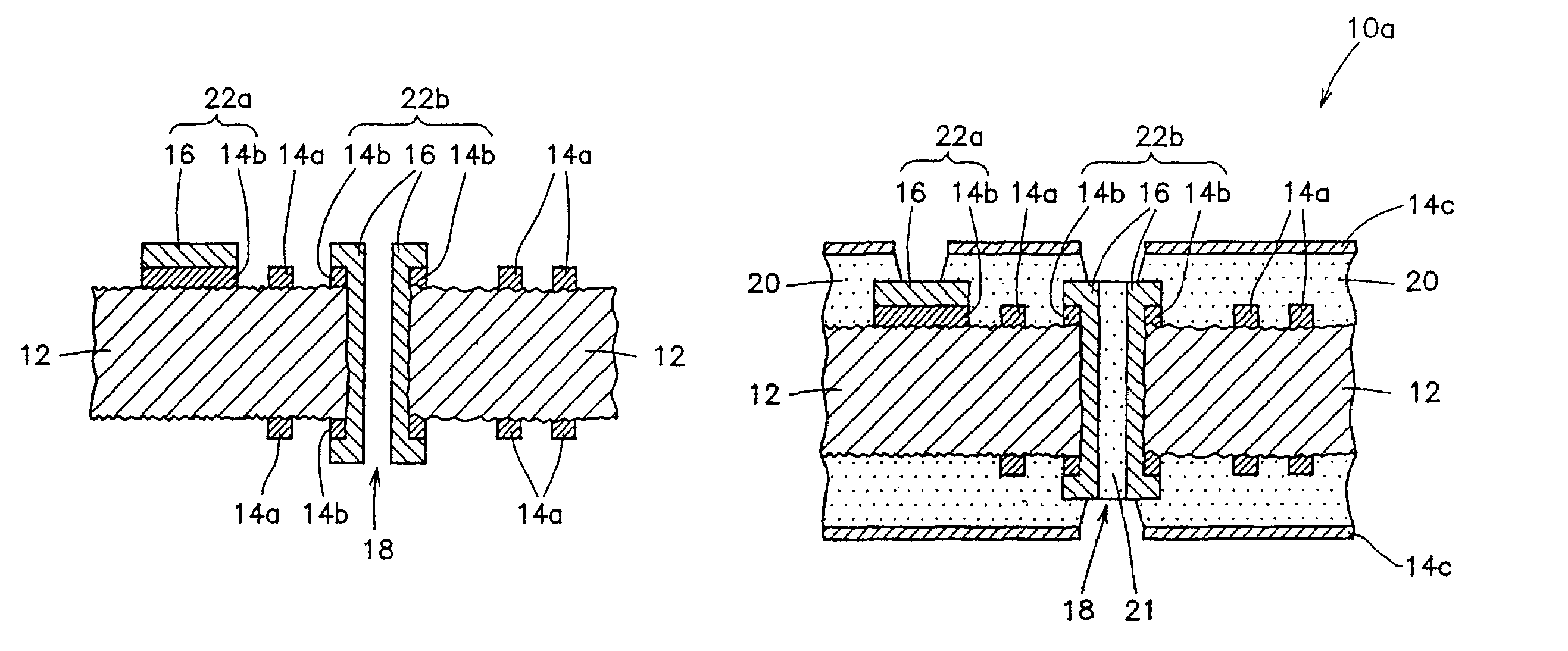
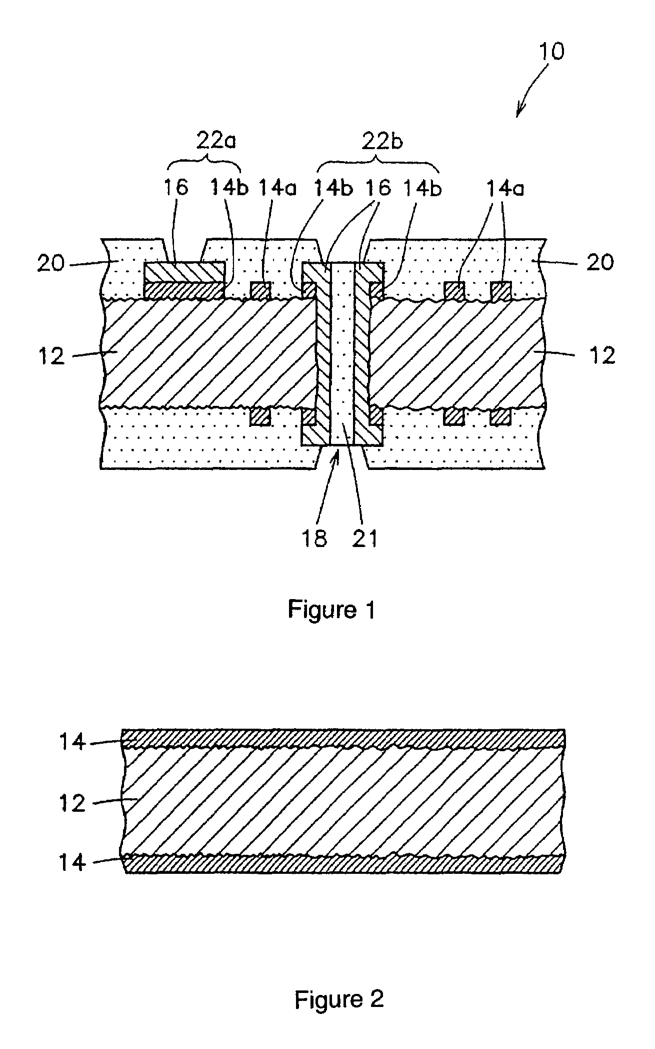
[0044]In a printed circuit board 10 shown in FIG. 1, lands 22a and 22b and lines 14a selectively formed on the front and back surfaces of an insulating substrate 12 differ in thickness from each other. The thickness of the lands 22a and 22b is larger than the thickness of the lines 14a. In the specification and the drawings, lands 22a represent via hole lands, while lands 22b represent through hole lands.

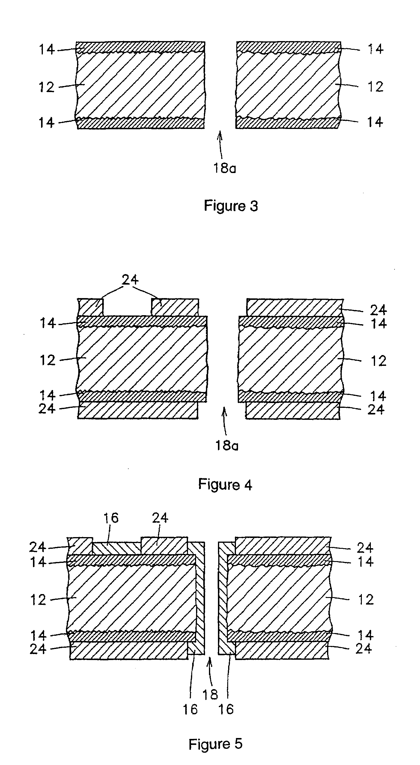
[0045]The lines 14a are formed by processing metal foil 14a on the insulating substrate 12v of the printed circuit board 10. The method of processing metal foil 14a is etching described below, or the like. Metal foil 14 is copper foil or the like. The lands 22a and 22b are formed of a stack of foil 14b and a plating layer 16 on the metal foil 14b. The plating layer 16 is formed by copper plating or the like.

[0046]A l...


PUM

PropertyMeasurementUnit
thicknessaaaaaaaaaa
thicknessaaaaaaaaaa
diameteraaaaaaaaaa

Abstract

The present invention provides a method of manufacturing a printed circuit board. The method includes the steps of preparing an insulating substrate having a front surface and a back surface and a layer of metal foil formed on each of the front surface and the back surface; selectively forming a plating layer for forming a land on at least one of the metal foils; adjusting a thickness of the plating layer; and forming the metal foils into lines.

Description

BACKGROUND OF INVENTION[0001]The present invention relates to a method of manufacturing a printed circuit board capable of adjustment of the aspect ratio of via holes and to a printed circuit board manufactured by the manufacturing method.[0002]In recent years, the pitch between terminals of semiconductor chips such as BGA (ball grid array) packages has been reduced. There is a need to reduce the pitch between lines / lands provided on printed circuit boards for mounting of semiconductor chips as well as to reduce the diameter of via / through holes.[0003]A land is a round or polygonal element of a circuit pattern provided on an insulating substrate for a printed circuit board. Terminals of a semiconductor chip are connected to lands, and via holes or through holes are formed in lands. Lines are portions of a circuit pattern other than lands.[0004]When lines are formed with a reduced pitch, it is desirable to reduce the thickness of the metal conductor layer. This is because if the thic...

Claims


Application Information

Patent Timeline
Patent Type & Authority Patents(United States)
IPC IPC(8): H01K3/10H05K3/06H05K3/10H05K3/42H05K3/46
CPCH05K3/427H05K3/064H05K3/108Y10T29/49165H05K2201/0959H05K2203/1394Y10T29/49155H05K3/4602
Inventor OHSUMI, KOHICHITERADA, KENJIYAMAZAKI, KOHICHI
Owner GLOBALFOUNDRIES U S INC
Learn More