CMOS-compatible bulk-micromachining process for single-crystal MEMS/NEMS devices

a micro-machining process and single-crystal technology, applied in the manufacture of microstructured devices, semiconductor devices, electrical equipment, etc., can solve the problems of requiring a larger dead-space around the device, requiring less accurate double-side polished wafers, and a higher risk of stiction of the device during processing and operation

Inactive Publication Date: 2010-07-06
SOLID STATE RES
View PDF20 Cites 7 Cited by
  • Summary
  • Abstract
  • Description
  • Claims
  • Application Information

AI Technical Summary

Problems solved by technology

However, this process uses polycrystalline SiGe instead of polycrystalline silicon.
Disadvantages include that the device's proximity to the substrate is defined by the insulator layer.
This subjects the device to a higher risk of stiction during processing and operation.
Disadvantages include a backside alignment which requires double-side polished wafers that is less accurate (front-to-back alignment) and which requires a larger dead-space around the device.
This also requires a long backside etch and results in a weaker wafer.
The material used for this is not single-crystal, resulting in poorer behaviors including lower Q when used for a resonant device.

Method used


Image

  • CMOS-compatible bulk-micromachining process for single-crystal MEMS/NEMS devices
  • CMOS-compatible bulk-micromachining process for single-crystal MEMS/NEMS devices
  • CMOS-compatible bulk-micromachining process for single-crystal MEMS/NEMS devices

Examples


Embodiment Construction

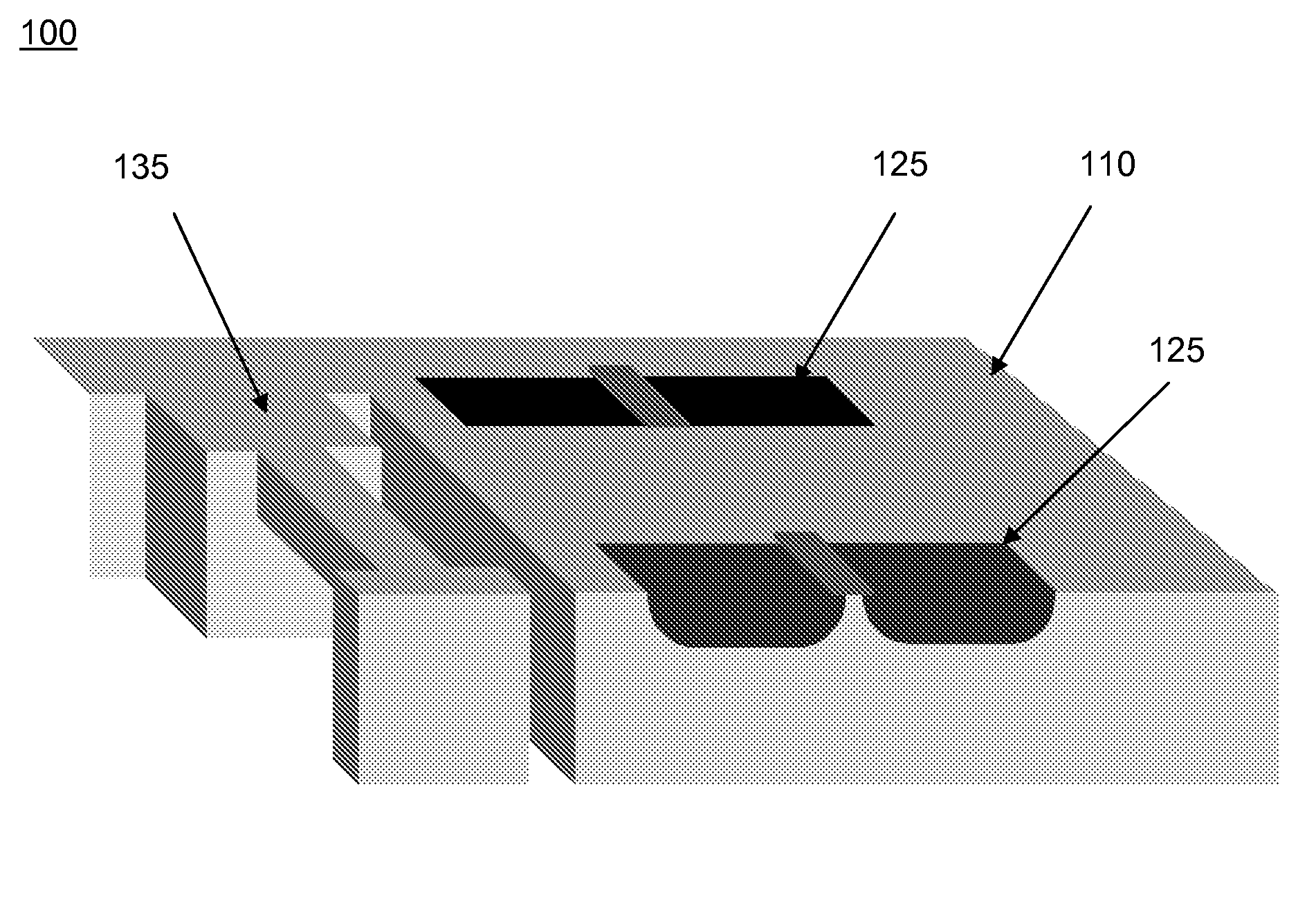
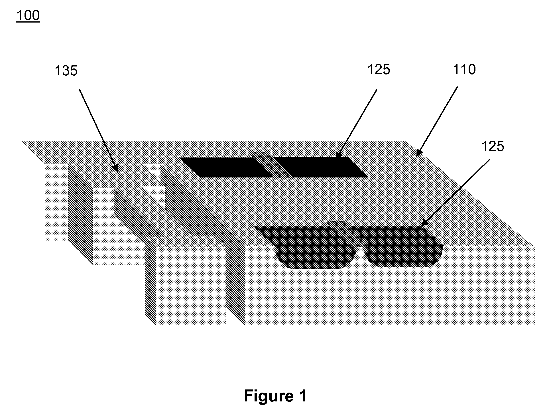
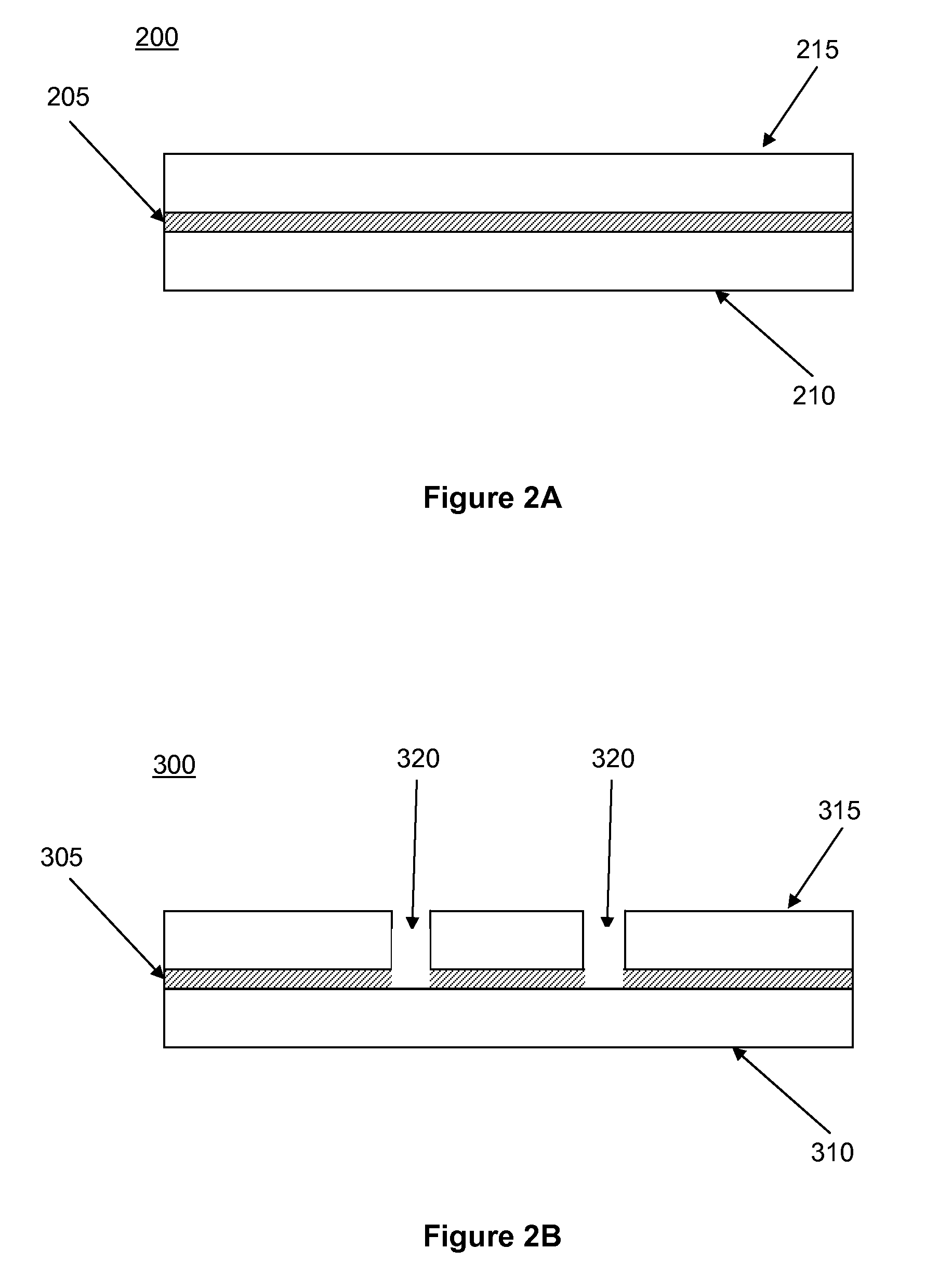
[0031]In one embodiment, begin with (1) a CMOS wafer with circuitry already fabricated. (2) Etch trenches to define MEMS structure using an anisotropic etch. During the etch, a protective layer is deposited simultaneously and remains only on the sidewalls of the etched cavity. In one embodiment, the etch could use sulfur hexafluoride (SF6) to etch the silicon and oxygen (O2) to form the protective layer on the sidewalls. In another embodiment, the protective layer is formed from a combination of O2, SiF4, and SF6. In another embodiment, the protective layer is SiO2 formed from an O2 plasma (plasma-enhanced oxidation). (3) The etch is either timed or stops on a middle layer (e.g. SOI) whose etch characteristics are different from that of the materials above and below. The middle layer can be formed, for example, by either pre-CMOS (e.g. bonded SOI, Separation by Implantation of Oxygen (SIMOX), etc.) or post-CMOS (SIMOX, ion implantation). (4) The middle layer is removed from the bott...


PUM

PropertyMeasurementUnit
temperatureaaaaaaaaaa
shapeaaaaaaaaaa
structureaaaaaaaaaa

Abstract

A process producing a single-crystalline device fabricated on a single-sided polished wafer employing processing from only the front-side and having a significant separation between the device and substrate is provided. In one embodiment, a method comprises an upper layer and a lower substrate. A device is formed in the upper layer, defined by gaps. The gaps are filled with at least one material that has etch characteristics different from those of the device and the substrate. At least a top portion of the gap material is removed from the upper layer. The gap material is etched so that a portion of the gap-material remains on the sidewalls of the surrounding upper layer. The material beneath the device is then etched, excluding an insulating layer beneath the device, releasing the device from the substrate. The insulating material beneath the device is then etched, the etch being selective to the insulating material and the gap material.

Description

FIELD OF THE INVENTION[0001]The invention relates to microelectromechanical systems (MEMS) and nanoelectromechanical systems (NEMS) device fabrication, including embodiments to processes producing a single-crystalline device fabricated on a single-sided or double-sided polished wafer employing processing from only one side and having a significant separation between the device and substrate.BACKGROUND OF THE INVENTION[0002]MEMS and NEMS technology continues to find new applications and employ multiple fabrication techniques. One known fabrication approach uses a high-temperature low pressure chemical vapor deposition (LPCVD) process to deposit polycrystalline silicon on top of a wafer with complementary metal-oxide-semiconductor (CMOS) circuitry. The polycrystalline silicon is then patterned to form a resonator.[0003]In another known approach, a resonator is made through bulk micromachining on a silicon-on-insulator (SOI) wafer. The insulating layer acts as an etch stop for the deep...

Claims


Application Information

Patent Timeline
Patent Type & Authority Patents(United States)
IPC IPC(8): H01L21/20
CPCB81C1/00246H01L27/0617H03H3/0072H03H9/2457B81C2203/0728
Inventor PAPAGEORGIOU, DEMETRIOS P
Owner SOLID STATE RES
Why Eureka
Try Eureka