Method of heat treatment of silicon wafer doped with boron

Inactive Publication Date: 2010-07-13
SUMCO TECHXIV
View PDF15 Cites 0 Cited by
  • Summary
  • Abstract
  • Description
  • Claims
  • Application Information

AI Technical Summary

Benefits of technology

[0022]In that case, the hydrogen heat treatment in the initial stage can be performed at a temperature in a range of, for example, 800° C. to 1200° C. For example, when the hydrogen heat treatment is performed at less than 800° C. while the temperature of the heat treatment furnace is being increased (e.g., hydrogen is added at 300° C., annealing in hydrogen is performed at 300° C. to 500° C., and switching to the argon atmosphere is made at 500° C.), it is not practical because an effect of removing boron from the wafer surface layer by annealing in hydrogen delays. Meanwhile, for example when the heat treatment in hydrogen is performed at a temperature exceeding 1200° C. while the temperature of the heat treatment furnace is being increased (e.g., hydrogen is added at 1210° C., annealing in hydrogen is performed at 1210° C. to 1300°

Problems solved by technology

When voids are exposed on the surface of the silicon wafer to form pits or, even if not exposed on the surface, when they are contained in the surface layer of the silicon wafer (i.e., when the COP is contained in a device activation area), they become a factor of causing a defect in the device properties, such as a defect in w

Method used


Image

  • Method of heat treatment of silicon wafer doped with boron
  • Method of heat treatment of silicon wafer doped with boron
  • Method of heat treatment of silicon wafer doped with boron

Examples


Example

Embodiment 1

[0053]Switching to hydrogen or gas containing hydrogen (argon dilution) was performed with timing as shown in Table 1, each gas was kept at each temperature for 24 minutes, and annealing in argon was continued at 1200° C.

[0054]The used wafer was a P-type (boron doped) with a diameter of 200 mm and having a resistivity of 10 to 20 (Ω·cm).

[0055]TABLE 1CZ wafer, 200 mm P-type, Resistivity: 10-20 (Ω· cm)LevelHydrogen addition temperature (° C.)Added hydrogen ratio (%)1800100280043100010041000451200100612004

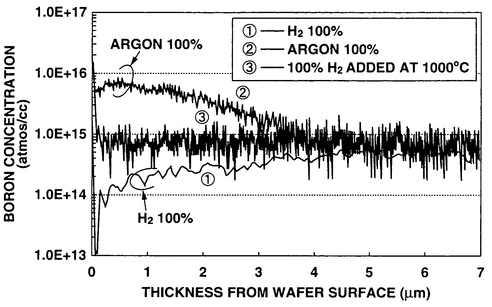
[0056]One example of the SIMS analysis results obtained by annealing is shown in FIG. 5. Fore comparison, FIG. 5 shows the boron concentration distribution after treating with argon only and the boron concentration distribution after treating with hydrogen only. It is seen from FIG. 5 that a boron concentration in the surface layer is uniformized by annealing in argon with hydrogen added in the initial stage of heat treatment.

[0057]Then, the boron concentration distributio...


PUM


Abstract

A method of subjecting a silicon wafer doped with boron to a heat treatment in an argon atmosphere, wherein the argon atmosphere is replaced with a hydrogen atmosphere or a mixed gas of an argon gas and a hydrogen gas in a proper fashion, to thereby uniformize a boron concentration in the thickness direction of the surface layer of the silicon wafer doped with boron.

Description

TECHNICAL FIELD[0001]The present invention relates to a method for a heat treatment of a silicon wafer doped with boron in an argon atmosphere, which is effective in uniformizing the boron concentration in the thickness direction of the wafer surface layer.BACKGROUND ART[0002]It is generally observed that a silicon wafer cut out from a dislocation-free silicon monocrystal ingot grown by the Czochralski (CZ) method has a crystal defect called COP (Crystal Originated Particle). The COP is caused by voids introduced during the ingot growing process. When voids are exposed on the surface of the silicon wafer to form pits or, even if not exposed on the surface, when they are contained in the surface layer of the silicon wafer (i.e., when the COP is contained in a device activation area), they become a factor of causing a defect in the device properties, such as a defect in withstand voltage in the gate oxide film or a defect in leak characteristic.[0003]In view of the circumstances descr...

Claims


Application Information

Patent Timeline
IPC IPC(8): H01L21/322H01L21/324C30B29/06H01L21/336
CPCH01L21/324H01L29/66507H01L21/3225H01L29/66477
Inventor SATO, YUJIYOSHINO, SHIROUFURUKAWA, HIROSHIMATSUYAMA, HIROYUKI
Owner SUMCO TECHXIV
Why Eureka
Try Eureka