Bandgap engineered MOS-gated power transistors

a technology of power transistors and mos-gated transistors, which is applied in the direction of sustainable manufacturing/processing, semiconductor devices, climate sustainability, etc., can solve the problems of large voltage transients at one or more device terminals, application can be very harsh, and the transistors are put under tremendous strain, so as to improve the immunity to transient voltages, reduce parasitic impedances, and improve the effect of immunity

Active Publication Date: 2010-07-13
SEMICON COMPONENTS IND LLC
View PDF23 Cites 8 Cited by
  • Summary
  • Abstract
  • Description
  • Claims
  • Application Information

AI Technical Summary

Benefits of technology

[0006]Accordingly, embodiments of the present invention provide devices, methods, and processes that improve immunity to transient voltages and reduce parasitic impedances.
[0007]Embodiments of the present invention provide transistors having improved immunity to unclamped inductive switching and other transient voltage events. For example, an exemplary embodiment of the present invention provides a trench-gated power MOSFET device having a SiGe source. A SiGe source reduces the gain of a parasitic npn transistor by reducing hole current in the body or well region, thereby decreasing the likelihood of a latch-up condition following an unclamped inductive switching event. The body tie on this device can also be eliminated in order to reduce transistor cell size.
[0008]Another exemplary embodiment of the present invention provides a trench-gated power MOSFET device having a SiGe body or well region. A SiGe body reduces hole current when the body diode is turned on, thereby reducing the power lost during its reverse recovery.
[0009]Embodiments of the present invention may also improve device characteristics. For example, an exemplary embodiment of the present invention reduces parasitic gate impedance by incorporating a poly SiGe gate. Another embodiment provides a channel having reduced channel resistance through the use of a SiGe layer near the device's gate.
[0010]Improvements that boost immunity to voltage transients and those that enhance device performance are not exclusive. For example, the use of a SiGe body decreases channel impedance, while a SiGe layer in the body region improves body diode reverse recovery. These embodiments may be used to improve n-channel or p-channel devices. Embodiments of the present invention may incorporate one of more of these or the other features described herein.

Problems solved by technology

These applications can be very harsh, putting a tremendous strain on these transistors.
For example, sourcing and sinking large currents into an inductive load can result in large voltage transients at one or more of the device's terminals.
Specifically, a large voltage excursion seen by a trench-gated power MOSFET can activate a parasitic npn transistor, leading to a destructive failure.
A less catastrophic, but still performance-degrading event, can occur when a large transient forward-biases a device's body diode, slowing the transistor's reverse recovery.
These inductive effects can limit the efficiency of a DC-to-DC converter, thereby wasting power.
Other limits on efficiency include the physical limitations of the trench-gated power MOSFETs themselves.
For example, parasitic impedances can cause power dissipation and heating of the devices.
Among these parasitic impedances is the series resistance of the gates of the devices.
While this series resistance can be mitigated using silicide, the efficacy of this procedure is limited due to the physical structure of these transistors.
Channel resistance, or Ron, also limits device performance, thus limiting converter efficiency.
Larger devices can reduce Ron, but this results in a more costly device.

Method used


Image

  • Bandgap engineered MOS-gated power transistors
  • Bandgap engineered MOS-gated power transistors
  • Bandgap engineered MOS-gated power transistors

Examples


Embodiment Construction

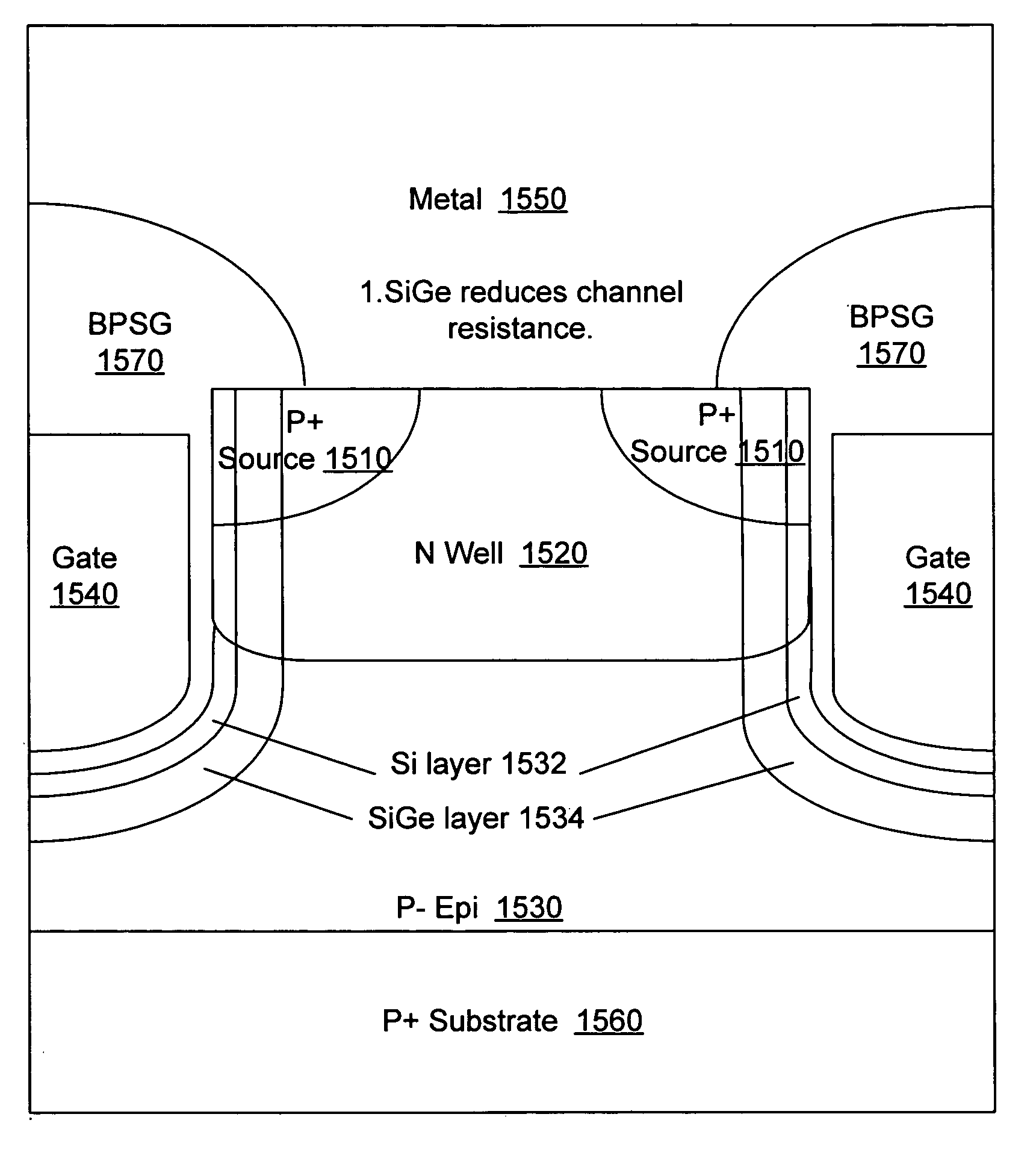
[0031]FIG. 1 is a cross section of an n-channel trench-gate power MOSFET that is improved by the incorporation of an embodiment of the present invention. This device includes n-type source regions 110, a body formed by p-well 120, n-type drain region 130, substrate 160, gates 140, and metal contact 150.

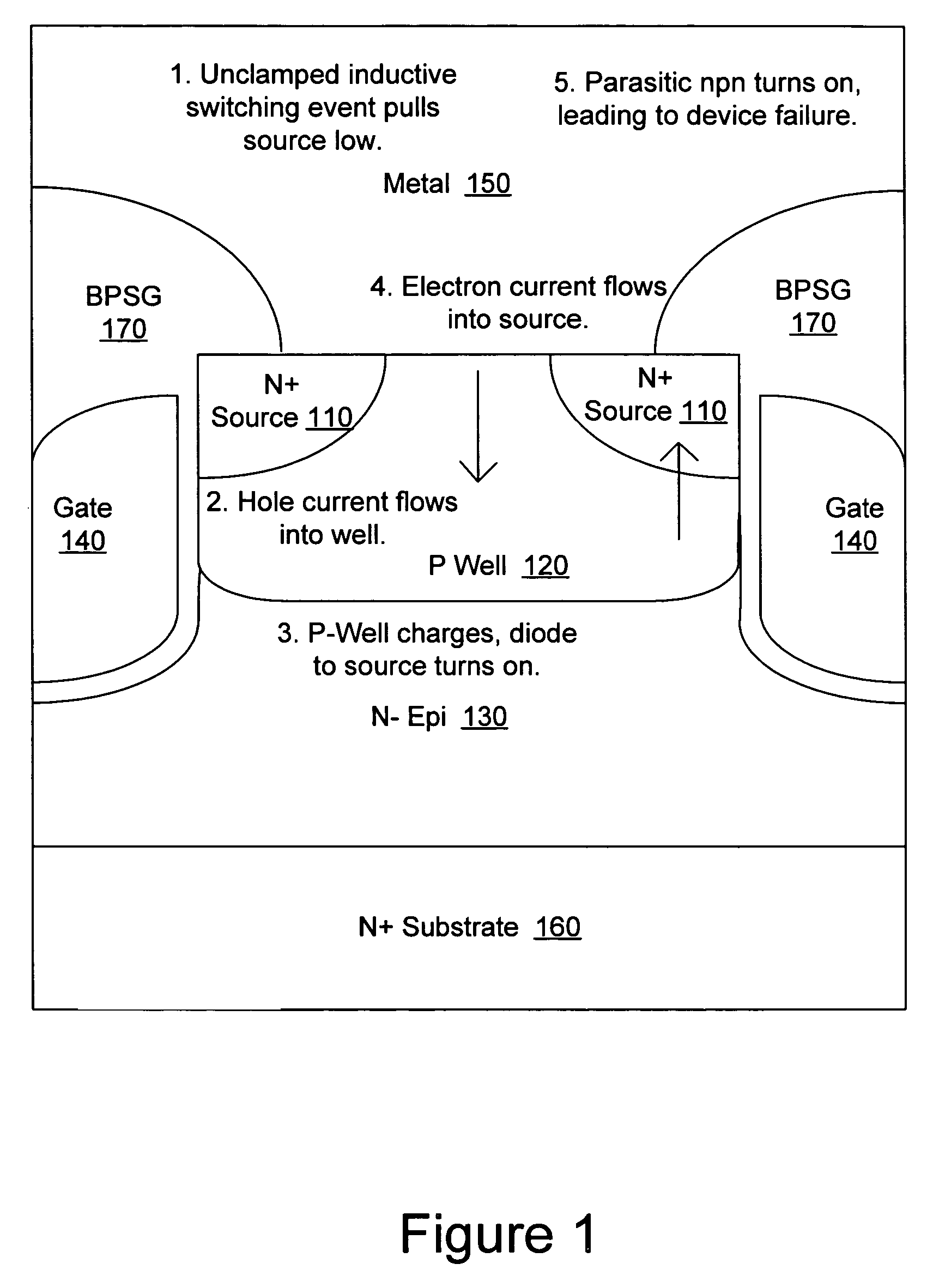
[0032]A parasitic npn bipolar transistor is inherent in this structure. Specifically, the parasitic device's emitter is the source region 110, its base is the body or well region 120, while the parasitic device's collector corresponds to the epi region 130. Destructive failure can occur if this parasitic transistor is biased into its forward active mode of operation. This can occur, for example, during avalanche breakdown induced by an unclamped inductive switching (UIS) event. Holes generated by impact ionization can flow through the base formed by the P-Well 120 causing an ohmic voltage drop. If this voltage drop exceeds about 0.6V, the turn-on voltage for the well-to-source junctio...


PUM


Abstract

Devices, methods, and processes that improve immunity to transient voltages and reduce parasitic impedances. Immunity to unclamped inductive switching events is improved. For example, a trench-gated power MOSFET device having a SiGe source is provided, where the SiGe source reduces parasitic npn transistor gain by reducing hole current in the body or well region, thereby decreasing the likelihood of a latch-up condition. A body tie on this device can also be eliminated to reduce transistor cell size. A trench-gated power MOSFET device having a SiGe body or well region is also provided. A SiGe body reduces hole current when the body diode is turned on, thereby reducing reverse recovery power losses. Device characteristics are also improved. For example, parasitic gate impedance is reduced through the use of a poly SiGe gate, and channel resistance is reduced through the use of a SiGe layer near the device's gate.

Description

[0001]This application claims the benefit of U.S. provisional application Nos. 60 / 617,167, 60 / 617,464, 60 / 617,463, and 60 / 617,168, each filed Oct. 7, 2004, each of which is incorporated by reference.BACKGROUND[0002]The present invention relates generally to power transistors, and more specifically to metal-oxide-semiconductor-gated (MOS-gated) power transistors with silicon-germanium (SiGe) sources, wells, channels, poly silicon-germanium gates, or a combination thereof.[0003]Trench-gated power MOSFET devices are popular choices for use in several demanding applications, such as DC-to-DC converters. These applications can be very harsh, putting a tremendous strain on these transistors. For example, sourcing and sinking large currents into an inductive load can result in large voltage transients at one or more of the device's terminals. Specifically, a large voltage excursion seen by a trench-gated power MOSFET can activate a parasitic npn transistor, leading to a destructive failure...

Claims


Application Information

Patent Timeline
Patent Type & Authority Patents(United States)
IPC IPC(8): H01L29/76
CPCH01L29/1054H01L29/165H01L29/49H01L29/7813H01L29/66734H01L29/4933H01L29/7782Y02P70/50
Inventor DOLNY, GARYWANG, QI
Owner SEMICON COMPONENTS IND LLC
Why Eureka
Try Eureka