Semiconductor device and manufacturing method thereof

a semiconductor and semiconductor technology, applied in the direction of semiconductor/solid-state device details, mechanical actuation of burglar alarms, instruments, etc., can solve the problems of increasing chip size, increasing cost per chip, and difficulty in maintaining circuit scale and antenna gain, so as to prevent signal attenuation due to shielded radio waves, less shielded, and the effect of reducing the diameter of the antenna

Inactive Publication Date: 2010-08-03
SEMICON ENERGY LAB CO LTD
View PDF91 Cites 41 Cited by
  • Summary
  • Abstract
  • Description
  • Claims
  • Application Information

AI Technical Summary

Benefits of technology

[0012]In addition, the wireless tag may be attached to a flexible material such as paper and plastic depending on the application, though the semiconductor substrate has a lower mechanical strength as compared with the aforementioned materials. Reduction in the area of the wireless tag itself allows the mechanical strength to increase to some extent. However, in that case, it is difficult to maintain the circuit scale and antenna gain. Particularly when the antenna gain is reduced, the communication distance is reduced and the application of the wireless tag is undesirably limited. Therefore, in view of the circuit scale of an IC chip and the antenna gain, the area of the wireless tag cannot be reduced randomly, leading to limit to the improvement of mechanical strength.
[0025]Without requiring a semiconductor substrate, the cost of the wireless tag can be drastically reduced. For example, the case of using a silicon substrate with a diameter of 12 inches is compared with the case of using a glass substrate with a size of 730×920 mm2. The silicon substrate has an area of about 73000 mm2 whereas the glass substrate has an area of about 672000 mm2, that is, the glass substrate is about 9.2 times as large as the silicon substrate. On the glass substrate with an area of about 672000 mm2, about 672000 wireless tags each having an area of 1 mm square can be formed when taking no account of margin for cutting the substrate, which is about 9.2 times as many as the wireless tags formed on the silicon substrate. In the case of using the glass substrate with a size of 730×920 mm2, which requires fewer manufacturing steps, the amount of capital investment in mass production of wireless tags can be reduced to one-third of that in the case of using the silicon substrate with a diameter of 12 inches. Further, according to the invention, after a thin film integrated circuit is peeled off from a glass substrate, the glass substrate can be reused. Therefore, the cost in the case of using the glass substrate can be significantly reduced as compared with in the case of using the silicon substrate, even taking into account the cost of repairing a broken glass substrate or cleaning a surface of the glass substrate. The invention also relates to a wireless tag in which a thin film integrated circuit formed on a substrate is not peeled off yet. In the case of shipping such a wireless tag before being peeled off, the cost of the glass substrate used as a material influences the cost of the wireless tag largely. However, the glass substrate with a size of 730×920 mm2 costs about half as much as the silicon substrate with a diameter of 12 inches.

Problems solved by technology

In the case of Patent Document 1, however, a guard band prevents high integration, and an increase in chip size is inevitable.
Since the cost per area of a semiconductor substrate is higher than that of a glass substrate, the increase in chip size leads to an increase in cost per chip.
However, in that case, it is difficult to maintain the circuit scale and antenna gain.
Particularly when the antenna gain is reduced, the communication distance is reduced and the application of the wireless tag is undesirably limited.
Therefore, in view of the circuit scale of an IC chip and the antenna gain, the area of the wireless tag cannot be reduced randomly, leading to limit to the improvement of mechanical strength.
Thus, there is a problem in that signals are easily attenuated depending on the direction of transmitted radio waves.

Method used


Image

  • Semiconductor device and manufacturing method thereof
  • Semiconductor device and manufacturing method thereof
  • Semiconductor device and manufacturing method thereof

Examples


embodiment 1

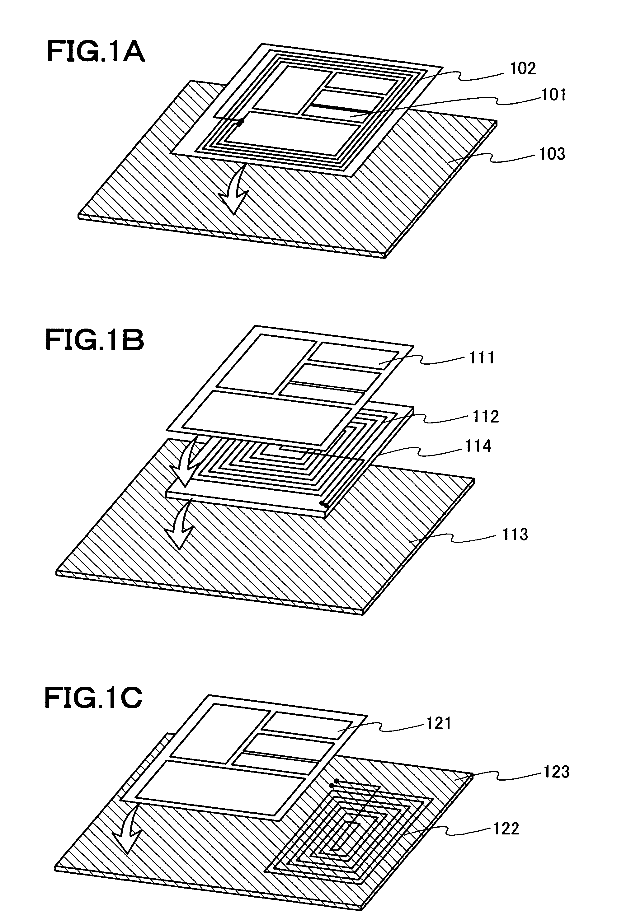
[0120]Described in this embodiment is an example of forming a plurality of wireless tags by using a large substrate.

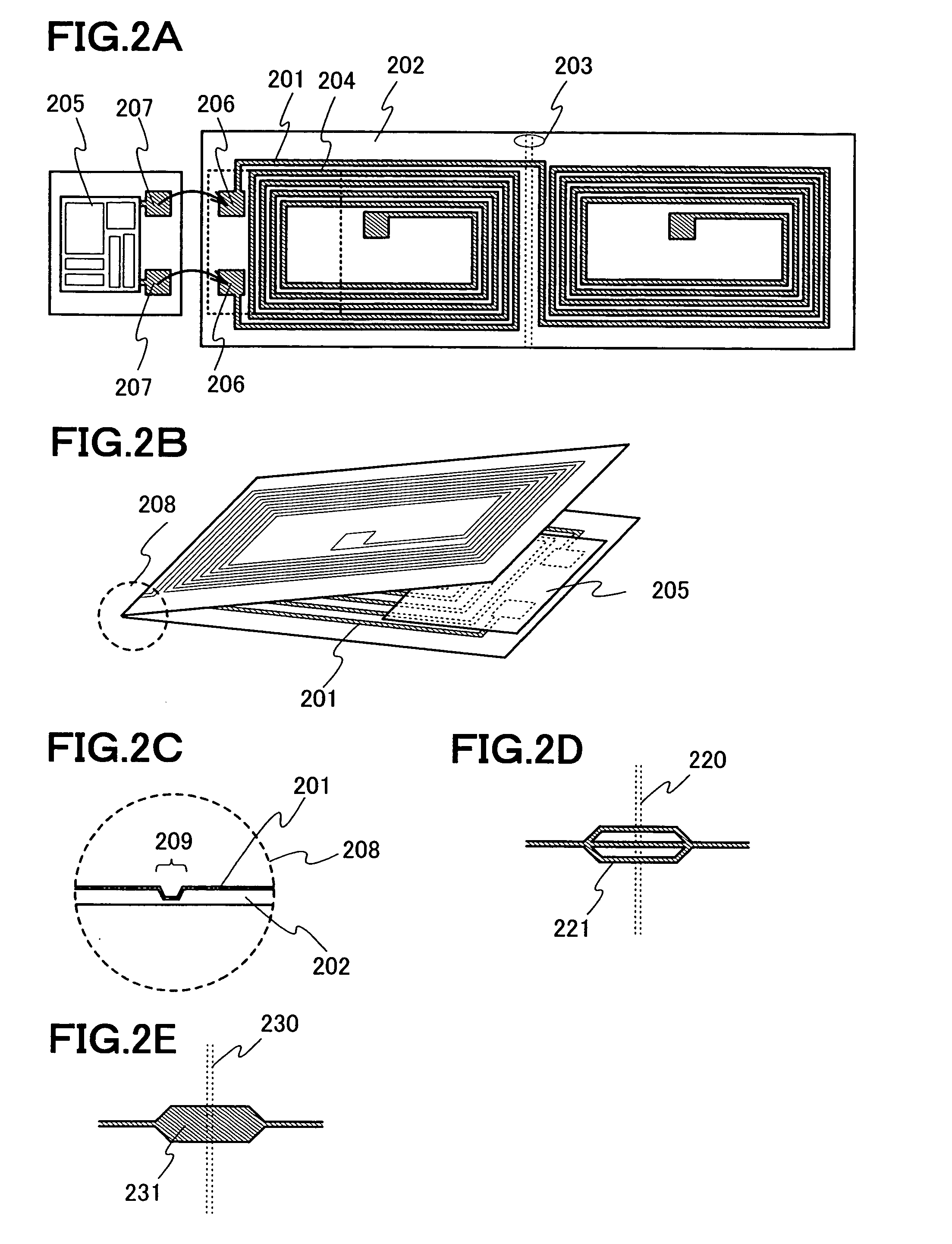
[0121]FIG. 10A shows a case in which a plurality of antennas 902 used for wireless tags are formed on a large flexible substrate 901 functioning as a support. At the same time, a plurality of thin film integrated circuits 903 are attached onto the flexible substrate 901 in FIG. 10A. When being attached, the thin film integrated circuits 903 are electrically connected to the antennas 902.

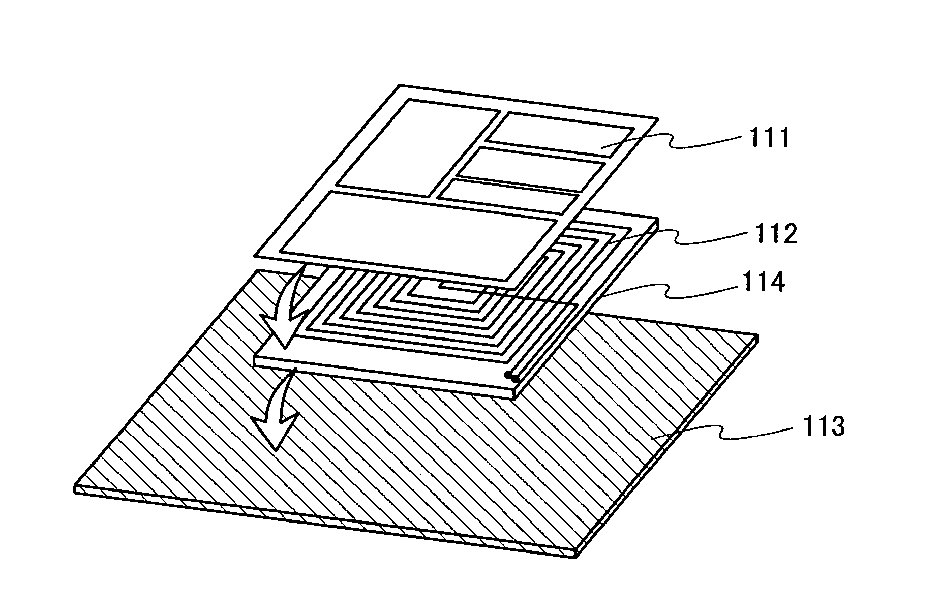
[0122]FIG. 10B shows a case in which the plurality of thin film integrated circuits 903 are attached onto the substrate 901. Although the antennas 902 and the thin film integrated circuits 903 are disposed to be adjacent to each other in FIG. 10B, the invention is not limited to this configuration. The antennas 902 and the thin film integrated circuits 903 may be overlapped to have a stacked structure.

[0123]Then, as shown in FIG. 10C, scribing or dicing is performed along a dashed line ...

embodiment 2

[0124]In this embodiment, applications of the wireless tag of the invention are described.

[0125]The wireless tag of the invention can be applied to various fields. For example, the wireless tag of the invention can be attached to a product label to control the flow of product.

[0126]As shown in FIG. 11A, a wireless tag 1102 of the invention is formed on a support with a sticky backside such as a seal 1101 and then attached to a product label 1103. Subsequently, as shown in FIG. 11B, the label 1103 attached with the wireless tag 1102 is put on a product 1104.

[0127]Identification data of the product 1104 can be wirelessly read from the wireless tag 1102 attached to the label 1103 as shown in FIG. 11C. Therefore, the wireless tag 1102 facilitates the control of product in the distribution process.

[0128]For example, in the case of a nonvolatile memory being used as a memory of a thin film integrated circuit in the wireless tag 1102, the distribution process of the product 1104 can be rec...

embodiment 3

[0130]In this embodiment, applications of the wireless tag of the invention are described.

[0131]When a thin film integrated circuit in the wireless tag of the invention includes a memory such as a ROM in which data cannot be rewritten, it is possible to prevent forgery of bills, checks, family registers, resident cards, traveler's checks, passports and the like. Further, when the wireless tag is used for foods whose commercial value depends crucially on a production area, a producer and the like, the forgery of production area, producer and the like can be prevented at low cost.

[0132]FIG. 13A shows an example of a check 1301 including a wireless tag 1302 of the invention. In FIG. 13A, the wireless tag 1302 is put inside the check 1301, though it may be exposed outside the check 1301.

[0133]FIG. 13B shows an example of a passport 1311 including a wireless tag 1312 of the invention. In FIG. 13B, the wireless tag 1312 is put on a cover of the passport 1311, though it may be put on other...


PUM

PropertyMeasurementUnit
frequenciesaaaaaaaaaa
diameteraaaaaaaaaa

Abstract

A semiconductor device typified by a wireless tag, which has improved mechanical strength, can be formed by a more simple process at a low cost and prevent radio waves from being shielded, and a manufacturing method of the semiconductor device. According to the invention, a wireless tag includes a thin film integrated circuit formed of an isolated TFT having a thin film semiconductor film. The wireless tag may be attached directly to an object, or attached to a flexible support such as plastic and paper before being attached to an object. The wireless tag of the invention may include an antenna as well as the thin film integrated circuit. The antenna allows to communicate signals between a reader / writer and the thin film integrated circuit, and to supply a power source voltage from the reader / writer to the thin film integrated circuit.

Description

BACKGROUND OF THE INVENTION[0001]1. Field of the Invention[0002]The present invention relates to a semiconductor device capable of communicating wirelessly and a manufacturing method of the semiconductor device.[0003]2. Description of the Related Art[0004]A semiconductor device typified by a wireless tag capable of wirelessly communicating identification data or the like has been put into practical use in various fields, and the market thereof is likely to further increase as a new type of communication information terminal. The wireless tag is also called an RFID (Radio Frequency Identification) tag or an IC tag. The wireless tag in practical use usually has an antenna and an IC chip formed by using a semiconductor substrate.[0005]An AC signal received by an antenna is rectified by a rectifier element such as a diode in a wireless tag, and then sent to the subsequent stages. In general, a transistor is used as the diode for rectification. A signal from the wireless tag can be read ...

Claims


Application Information

Patent Timeline
Patent Type & Authority Patents(United States)
IPC IPC(8): G08B13/14G06K19/07H01L21/30H01L21/77H01L21/84H01L27/02H01L27/12H01L29/786
CPCH01L27/1214H01L29/78603H01L27/1266Y10T29/49117H01L27/1218
Inventor YAMAZAKI, SHUNPEIKOYAMA, JUNAKIBA, MAI
Owner SEMICON ENERGY LAB CO LTD
Why Eureka
Try Eureka