Method for fabricating piezoelectric element

a piezoelectric element and manufacturing method technology, applied in piezoelectric/electrostrictive transducers, device material selection, transducer types, etc., can solve the problem of limited applicability, achieve uniform solvent vapor flow, reduce masking agent reflow, and improve applicability

Inactive Publication Date: 2010-08-10
JAPAN SCI & TECH CORP
View PDF21 Cites 5 Cited by
  • Summary
  • Abstract
  • Description
  • Claims
  • Application Information

AI Technical Summary

Benefits of technology

[0010]The inventors have further continued researches and examinations on thickness distribution of masking agent, which is applied to a surface of piezoelectric material, and discovered a peculiar behavior of the masking agent. Namely, when the masking agent, applied to the piezoelectric material, is re-dissolved in contact with a solvent vapor, it rises upwards due to a surface tension. The reflow motion of the masking agent is effective for control of thickness distribution.
[0011]A major object of the present invention is to easily impart predetermined thickness distribution to a masking film without any dimensional restriction. Another object of the present invention is to provide piezoelectric elements with surface profiles corresponding to thickness distribution of the masks.
[0014]When a masking agent such as a photoresist is applied onto a surface of piezoelectric material and then fluidized by contact with a stream of a solvent vapor, the masking agent is raised upwards to a convex shape with predetermined thickness distribution. The thickness distribution is advantageous for reforming a surface of the piezoelectric material to a domed shape with a curvature radius within a range of several micrometers to several centimeters, i.e. high applicability to various scales in comparison with a conventional thermal reflow process. A flow rate of the solvent vapor is controlled by supplying a solvent, which is diluted by an inert gas such as nitrogen, and a uniform flow of the solvent vapor is ensured by use of a shower head.
[0015]Piezoelectric material, which has a surface partially subjected to oil-repelling treatment, restricts reflow of a masking agent to the other surface part or parts. Restriction of the reflow motion enables formation of one or more domed masks with predetermined thickness distribution on predetermined surface parts of the piezoelectric material. By dry etching the piezoelectric material together with domed masks, the surface parts coated with the domed mask are processed to three-dimensional shapes corresponding to the thickness distribution of the domed masks. In short, the present invention is employable for fabrication of multi-channeled piezoelectric devices, wherein a plurality of piezoelectric elements are arranged with a predetermined pattern, useful as upgraded sensors.

Problems solved by technology

The other process, wherein predetermined thickness distribution is imparted to a resist film by controlling an energy of light, is extremely expensive for deposition of a desired mask in comparison with a conventional process, so that its applicability is limited from an economical point of view.

Method used


Image

  • Method for fabricating piezoelectric element
  • Method for fabricating piezoelectric element
  • Method for fabricating piezoelectric element

Examples


example

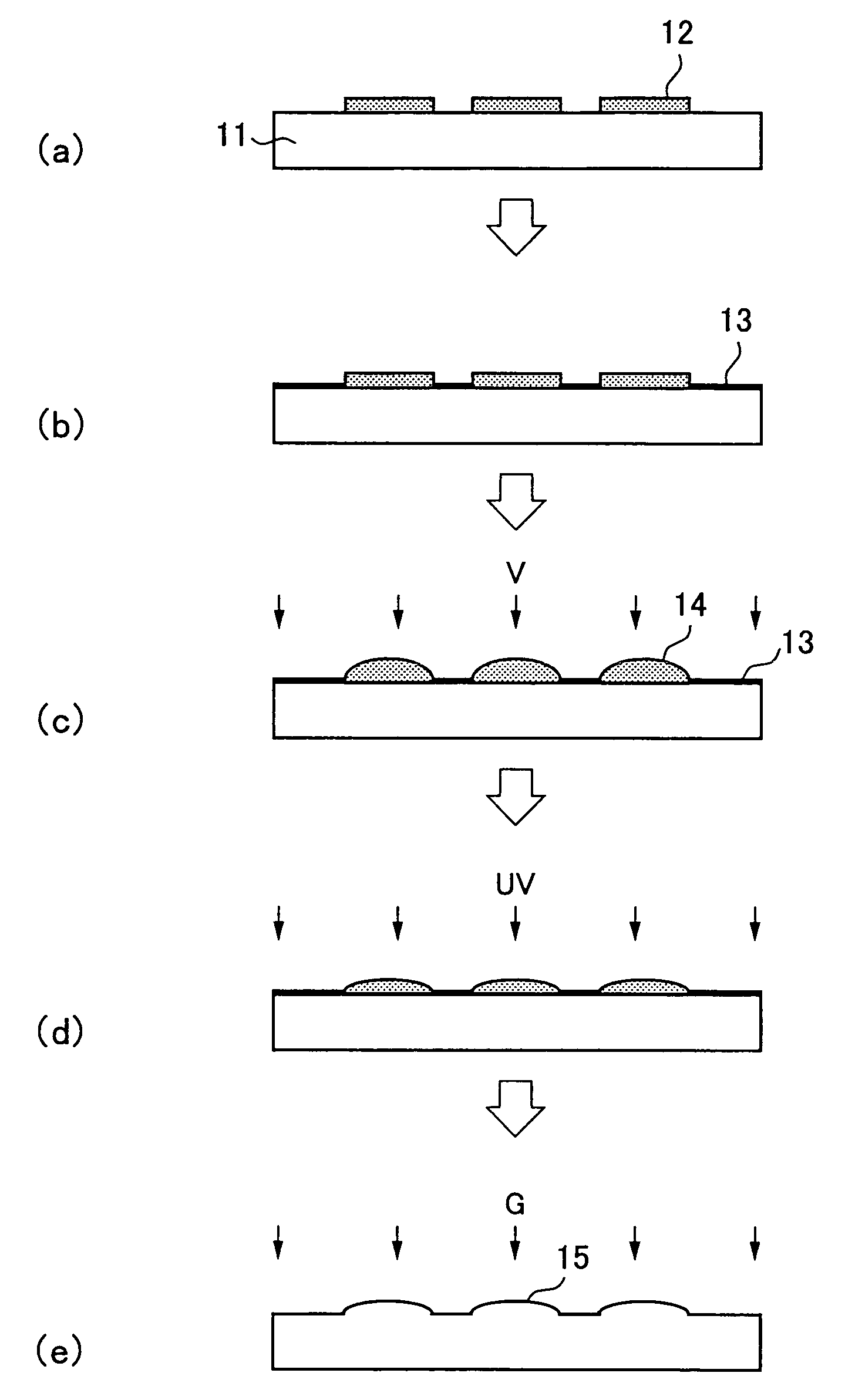
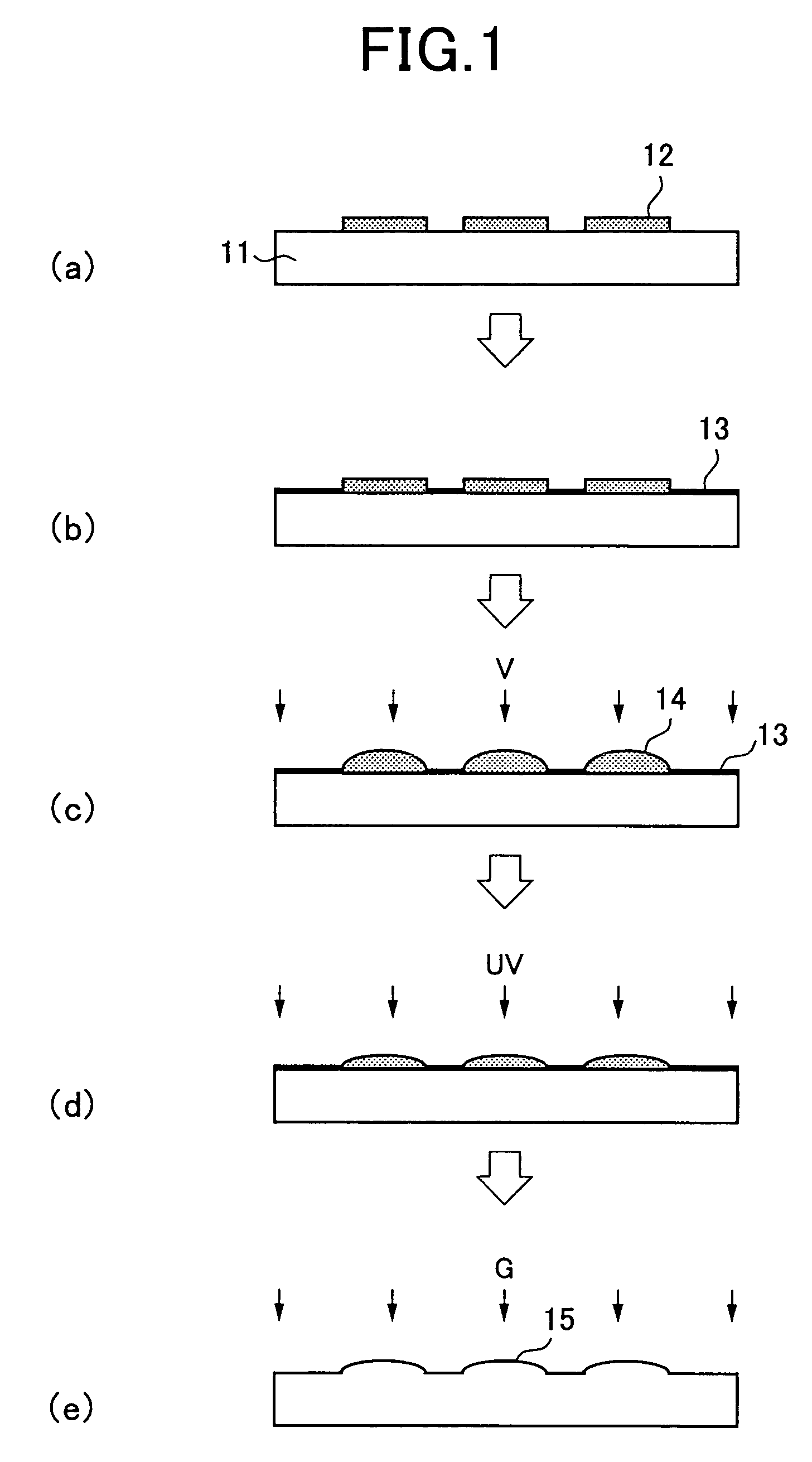
[0030]AT cut quartz of 100 μm in thickness was provided as a substrate 11. A solvent vapor V was prepared by heating propylene glycol monomethyl ether acetate (PGMEA), i.e. a solvent specialized for a photoresist AZP4400 (offered by Clariant Co., Ltd.), at 75° C. or higher, and bubbling the solvent with a nitrogen gas.

[0031]The photoresist was applied as a masking agent to the substrate 11 by a spinner, so as to deposit a masking film 12 of 6 μm in average thickness on the substrate 11. After the masking film 12 was shaped to a predetermined pattern by photolithography, hexamethyldisilazane (HMDS) was applied as a surface treatment chemical 13 to a surface part of the substrate 11, in order to reduce a surface tension of the substrate 11, which was not coated with the masking film 12.

[0032]After the surface of the substrate 11 was dried, the substrate 11 was located on a stage inside a chamber and held at a room temperature or so. The solvent vapor V was introduced onto the surface ...


PUM

PropertyMeasurementUnit
diameteraaaaaaaaaa
diameteraaaaaaaaaa
diameteraaaaaaaaaa

Abstract

A piezoelectric element is manufactured by applying a masking agent to a surface of a piezoelectric material to form a film of the masking agent on the surface of the piezoelectric material. The film of the masking agent is patterned into a masking pattern. Oil repellent is selectively applied to surface portions of the substrate which are not covered with the patterned film. The patterned film is held in contact with a vapor of a solvent for the masking agent, diluted with an inert gas, to fluidize the film to a domed shape on the surface of the piezoelectric material. The diluted vapor is formed by bubbling the solvent with the inert gas. The dome-shaped film is then cured and the piezoelectric material is dry etched together with the cured film to process the piezoelectric material into a three-dimensional convex profile corresponding to the thickness distribution of the domed shape.

Description

BACKGROUND OF THE INVENTION[0001]1. Field of the Invention[0002]The present invention relates to a method of manufacturing piezoelectric elements, which have three-dimensional surfaces for distribution of big masses at centers.[0003]2. Description of Related Art[0004]Piezoelectric elements, represented by quartz oscillators, have been used in various fields such as oscillation sources of standard frequency and clocks of electronic or electrical devices. Recent researches and developments are focused on how to reduce thickness of piezoelectric material and how to shape piezoelectric material to lenticular profiles for advanced performance of data processing or transmission capability.[0005]As for large-scaled oscillators with electrodes of several millimeters or more in diameter, piezoelectric material is etched to domed shapes by a wet process and then dressed to profiles with curved surfaces by mechanically polishing edges of the domed shapes. As for small-scaled oscillators with e...

Claims


Application Information

Patent Timeline
Patent Type & Authority Patents(United States)
IPC IPC(8): H01L41/22H04R17/00H01L21/3065H01L41/08H01L41/09H01L41/18H01L41/332H03H3/02H03H9/19
CPCH03H3/02H01L41/332Y10T29/42Y10T29/435H10N30/082H10N30/081
Inventor ABE, TAKASHILI, LI
Owner JAPAN SCI & TECH CORP
Why Eureka
Try Eureka