Wave absorber

a technology of absorber and wave, applied in the direction of electrical equipment, individually energised antenna arrays, antennas, etc., can solve the problems of deterioration of communication quality, increased weight, and need for more thickness, so as to reduce weight, thin thickness, and thin size

Inactive Publication Date: 2010-08-17
MITSUBISHI GAS CHEM CO INC
View PDF52 Cites 5 Cited by
  • Summary
  • Abstract
  • Description
  • Claims
  • Application Information

AI Technical Summary

Benefits of technology

[0020]The present invention is aimed to solve the aforementioned problems of the prior arts. Objects of the present invention are to provide a wave absorber which has a reflection-attenuating capability to prevent communication failure due to reflection of an electromagnetic wave, can be thin-sized and reduced in weight, and has low property variation according to the incident angle of the wave.

Problems solved by technology

However, in this case, a radiated wave from a communication device itself remains in a room due to reflection, and this reflected wave and a desired communication radio wave can be interfered, thereby causing deterioration of communication quality.
However, in the wave absorber described in Patent Document 1, which is produced by mixing and dispersing a magnetic powder such as ferrite or a soft magnetic metal in an insulative matrix such as a rubber or a plastic followed by molding, it is possible to form a relatively thin absorber, but there are the drawbacks that a more thickness is necessary when high-performance wave absorption is required, and there is a problem in that the weight increases due to use of material of high specific gravity.
Therefore, there are problems in that the wave absorber should be pyramid-shaped or wedge-shaped or that the thickness should be large along the absorption direction, in order to obtain the desired performance.
However, a wave absorber described in Patent Document 3 requires a thickness of λ / 4 at a certain frequency in principle, and has a problem in that a radio wave absorption property varies according to the incident angle of the wave.
However, this wave absorber has a problem in that a radio wave absorption property (frequency) varies according to the incident angle of the wave as in the case of the λ / 4 type.
Therefore, the wave absorber has a problem in property variation during production.

Method used


Image

  • Wave absorber
  • Wave absorber
  • Wave absorber

Examples


first embodiment

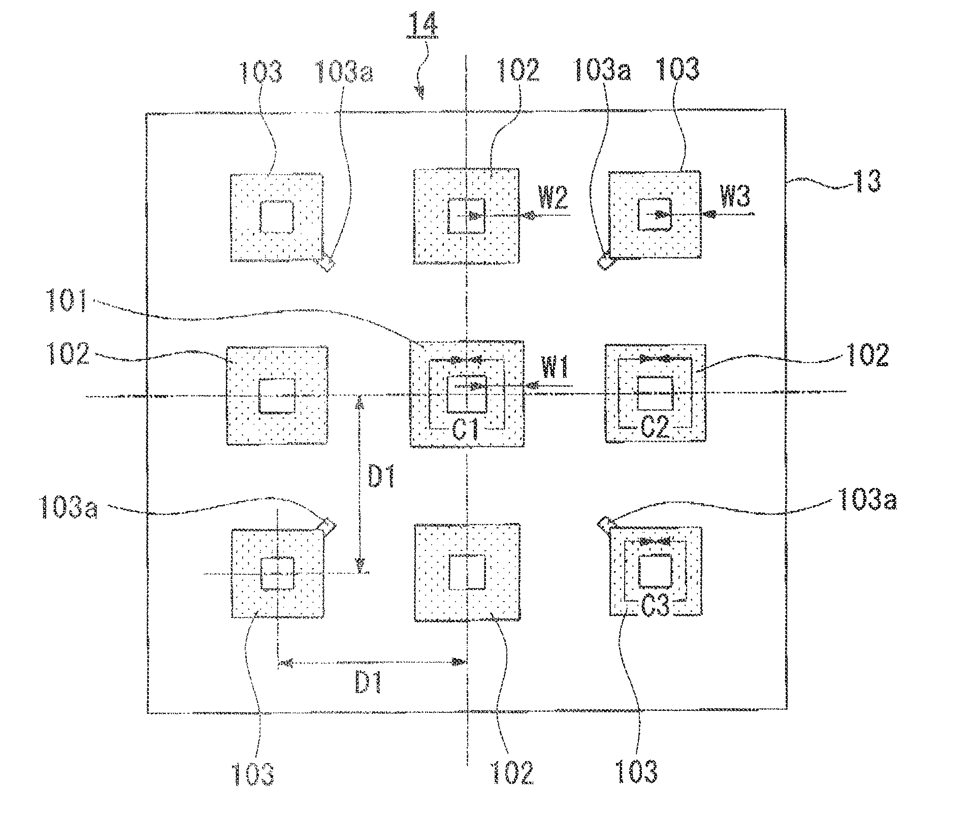
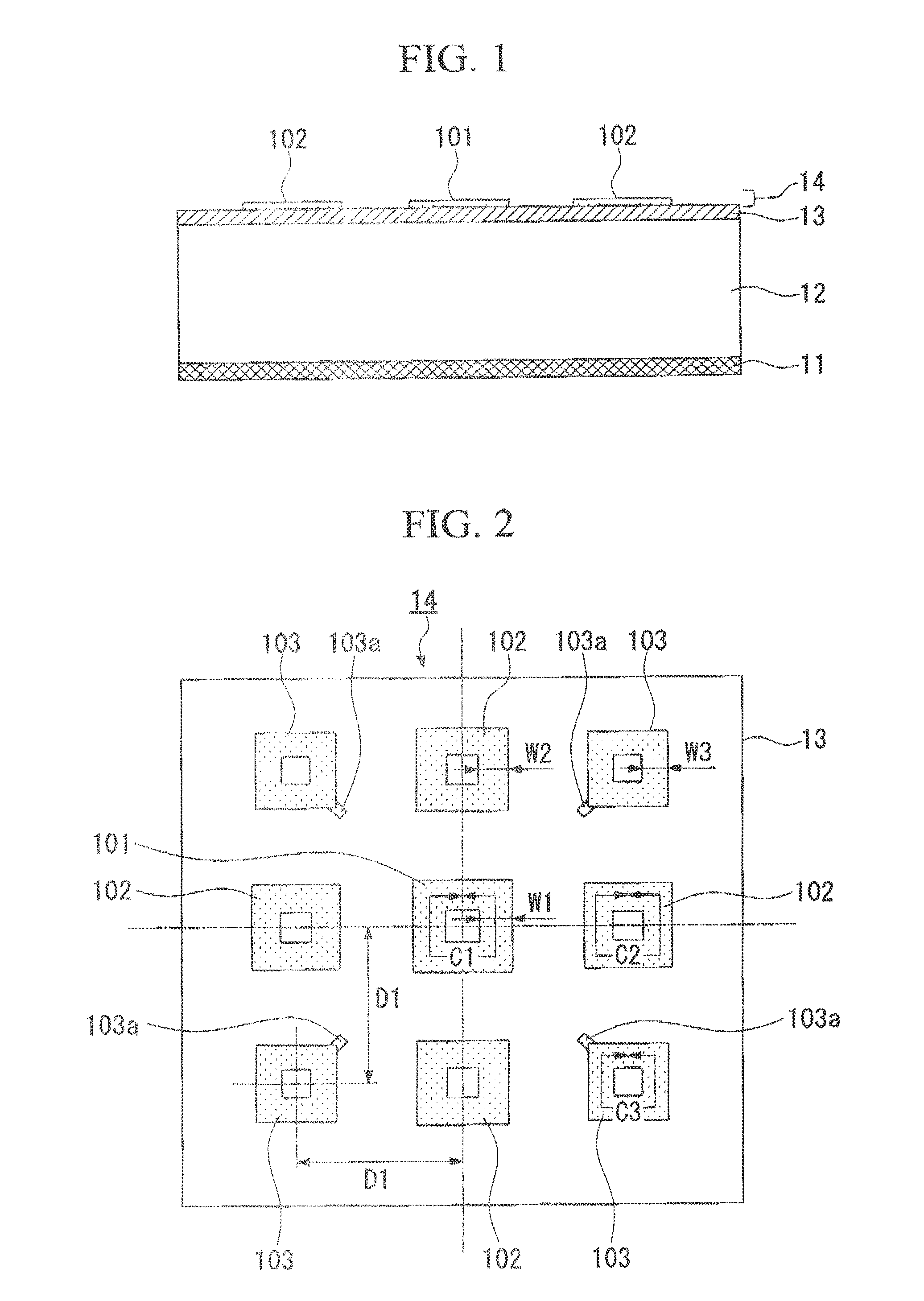
[0100]FIG. 1 is a cross-sectional view showing schematic features of a wave absorber of the first embodiment of the present invention. A wave absorber of the present embodiment includes a sequentially laminated structure including a conductor layer (11) formed of a copper foil having a thickness of 18 μm; a PC (polycarbonate) substrate (12) having a thickness of 2.0 mm, which forms a first dielectric layer A; a BT (bismaleimide-trazine) substrate (13) having a thickness of 0.3 mm, which forms a first dielectric layer B; and a patterned layer (14) in which a plurality of loop patterns, which is formed of a copper foil and is different with respect to a shape thereof, is placed periodically.

[0101]FIG. 2 is a plan view of the wave absorber illustrated in FIG. 1, and shows detailed features of a patterned layer (14). The patterned layer (14) includes a plurality of loop patterns (101, 102, and 103) formed on the upper surface of the BT substrate (13). Each of loop patterns (101, 102, an...

second embodiment

[0111]FIG. 4 is a cross-sectional view showing schematic features of a wave absorber of the second embodiment of the present invention. A wave absorber of the present embodiment includes a sequentially laminated structure including a grating-shaped conductor layer (21) formed by using a conductive mesh cross; a PC (polycarbonate) substrate (22) having a thickness of 3.7 mm, which forms a first dielectric layer A; a PET (polyethylene terephthalate) substrate (23) having a thickness of 0.1 mm, which forms a first dielectric layer B; a patterned layer (24) in which a plurality of loop patterns, which is formed of ITO (Indium Tin Oxide) having a surface resistivity (sheet resistance) of 10 [Ω / □] and is different with respect of a shape thereof, is placed periodically; and a PC substrate (25) having a thickness of 0.3 mm.

[0112]Herein, a grating-shaped conductor layer (21) is formed with a line width of about 30 μm and a central line spacing of 0.254 mm, and has a function to totally refl...

third embodiment

[0118]FIG. 7 is a cross-sectional view showing schematic features of a wave absorber of the third embodiment of the present invention. A wave absorber of the present embodiment includes a sequentially laminated structure including a grating-shaped conductor layer (32) formed by screen printing using a conductive silver plate on a PET substrate (31) as a second dielectric layer A; a PC substrate (33) having a thickness of 3.2 mm, which forms a first dielectric layer A; a PET substrate (34) having a thickness of 0.1 mm, which forms a first dielectric layer B; a patterned layer (35) in which a plurality of loop patterns, which is formed of ITO having a surface resistivity (sheet resistance) of 10 [Ω / □] and is different with respect to a shape thereof, is placed periodically; and a PC substrate (36) having a thickness of 0.3 mm.

[0119]Herein, a grating-shaped conductor layer (32) is formed with a line width of about 100 μm and a central line spacing of 1.4 mm, and has a function to total...


PUM


Abstract

A wave absorber of the present invention includes a sequentially laminated structure including an conductor layer (11) made of a conductive material; a first dielectric layer (polycarbonate substrate (12) and bismaleimide-triazine substrate (13)) made of one layer or a multilayer of a dielectric material; and a patterned layer (14) including a plurality of a pattern made of the conductive material, wherein the conductor layer, the first dielectric layer, and the patterned layer are laminated sequentially, and each pattern in the patterned layer (14) is different from other adjacent patterns with respect to at least one of size and shape. Therefore, the wave absorber has sufficient reflection-attenuating capability to prevent communication failure caused by a reflection of a radio wave and so on, can be thin-sized and reduced in weight, and has a wide-band attenuation property.

Description

TECHNICAL FIELD[0001]The present invention relates to a wave absorber. Also, the present invention relates to a method for absorbing waves and a wave absorber which is capable of preventing communication failure due to reflection of electromagnetic (EM) waves and the like and of being thin-sized and reduced in weight.[0002]Priority is claimed on Japanese Patent Application No. 2004-258182, filed Sep. 6, 2004, the content of which is incorporated herein by reference.BACKGROUND ART[0003]In recent years, development of wireless communication systems including a mobile telephone, a wireless LAN (Local Area Network), and ITS (Intelligent Transport Systems) has caused the need for protection of communication information and for prevention of radio interference and false communication. When the main purpose is protection of communication information, each of indoor and outdoor radio waves is isolated by using an electromagnetic wave-shielding material so as to shield each of a foreign radi...

Claims


Application Information

Patent Timeline
Patent Type & Authority Patents(United States)
IPC IPC(8): H01Q17/00
CPCH01Q15/14H01Q17/00H01Q15/0026H05K9/0088H01Q15/0013H01Q19/10H01Q21/06
Inventor MASUDA, YOSHIYUKIOTANI, NOBORUNAKANO, HISAMATSU
Owner MITSUBISHI GAS CHEM CO INC
Why Eureka
Try Eureka