
Decentralised fault-tolerant clock pulse generation in VLSI chips

a clock pulse and fault-tolerant technology, applied in the direction of generating/distributing signals, pulse techniques, instruments, etc., can solve the problems of increasing the power consumption of the clock tree, the insufficient selection of low-tolerance quartz crystals alone, and the inability to control the clock pulse distribution. to achieve the effect of enhancing the stability of the global system clock puls

Inactive Publication Date: 2010-09-07
VIENNA UNIVERSITY OF TECHNOLOGY
View PDF12 Cites 9 Cited by
  • Summary
  • Abstract
  • Description
  • Claims
  • Application Information

AI Technical Summary

Benefits of technology

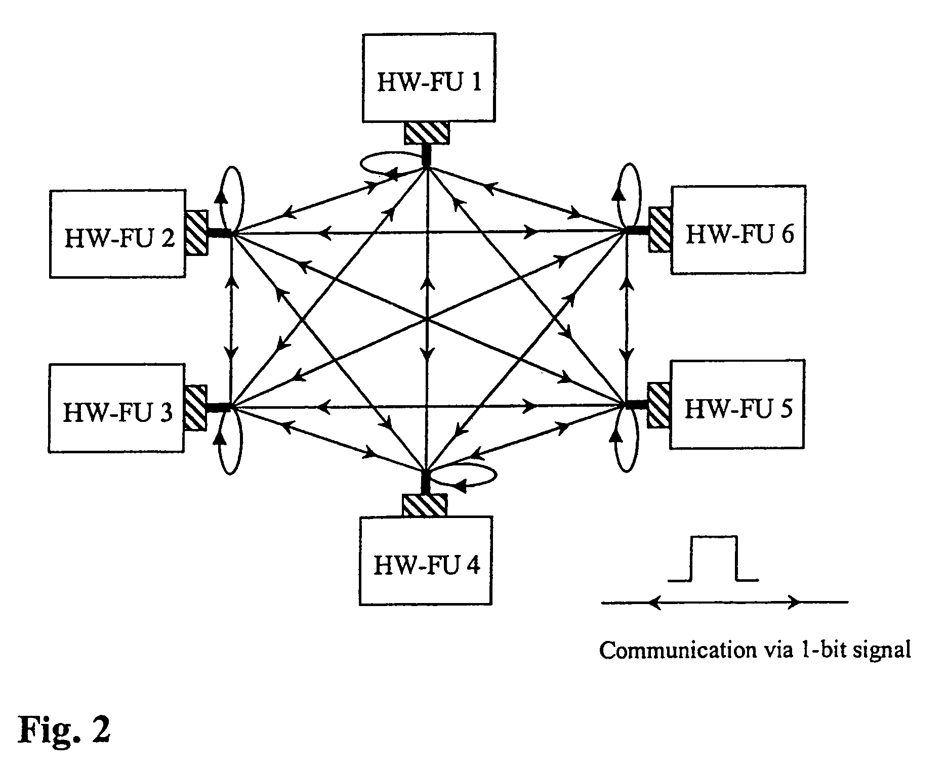
The invention is about a method for generating a global system clock pulse in hardware systems without using external or internal clock oscillators. The method involves a plurality of intercommunicating fault-tolerant clock pulse synchronization algorithms, which exchange information via a user-defined and permanent network of clock pulse signals. Each algorithm is assigned to one or more functional units, and their local clock pulses are synchronized with a global clock pulse. The global system clock pulse is derived from any local clock pulse with a specified frequency. The method is robust against transient and permanent faults and can ensure synchronization accuracy during power-up phase and data transmission. The invention also includes a hardware system carrying the method.

Problems solved by technology

The selection of low-tolerance quartz crystals alone would not be adequate, since the local clock times derived from them can deviate widely from one another over a longer period of time.
The clock pulse distribution in current designs represents an ever-increasing problem on account of the specifications for the performance and power consumption.
The demand for high clock frequencies and the increasing number of gates on microchips imply an increase in the power consumption of the clock tree owing to the enhanced number of switching operations and the high fan-out.
Each buffer has a certain, though slight, degree of inaccuracy with respect to its driving power and delay characteristics as a result of the manufacturing process that leads to additional clock skew [Restle01].
Moreover, the resistance of a line can, for example, change as a result of electro-migration, which can lead to changed execution time characteristics for this path.
Owing to the high frequencies (GHz range), the skin effect (current flows only on the surface of the conductor) is also becoming more of a problem [Chen02].
The inaccuracies of the parameters demonstrated above make it necessary to plan large margins of safety for the clock skew, which leads to substantial reduction in the maximum permissible clock frequency of a VLSI chip.
Moreover, the synchronous switching of many clock buffers generates considerable interference signals in the power supply, crosstalk and low-band electromagnetic interference radiation, which can be substantial as a result of the antenna effect of the clock tree.
In the case of consistency-based algorithms too it must be possible to assign the messages to the senders uniquely; in addition, many rounds of information exchange must take place so that the same global picture of the system is achieved in each zero-error node, which leads to very high overheads in terms of messages.
Furthermore, probabilistic methods can only be used meaningfully in software solutions, since the hardware costs for the implementation of the statistical tests and storage of the required data would be immense.
Under practical conditions this assumption cannot be maintained since, as already explained in the section on clock pulse distribution, the problems of the clock skew and the signal execution times become increasingly predominant.
An approach to compensating the different execution times has been shown by [Shin88], but, however, this requires 2n phase detectors and 2n2 leads, which further increases the hardware costs and the susceptibility to errors.
Owing to the phase shift of individual clock pulse edges there can not only be inconsistencies with the voters, but far more, there could be meta-stability problems at the voter inputs of individual nodes, since signal changes can also occur during the setup and hold times of the respective input flip-flop.
The probability of meta-stability problems can, of course, be reduced, but not completely ruled out, with the use of special input buffer circuits, which does not represent a conceptually elegant solution.
If the input signal of a PLL shows large deviations from the reference signal, then the PLL cannot regulate the signal successfully, which can lead to permanent loss of synchronization.
While the GALS technique enables the continued and unchanged use of proven synchronous design methods within a functional unit, fundamental problems occur exactly at the interfaces to the asynchronous communication units.
These synchronizers are mostly based on pausable / strechable clocks and lead to substantial delay times at the asynchronous / synchronous interface [Chelcea00].
Another serious problem with the GALS approach is that the local clock pulses work completely unsynchronized and can, thus, drift apart from each other at random.
Hence, it is not possible to establish a temporal ordering of the information exchanged without taking any additional measures.
As a result, the GALS approach can be used practically, but, however, in its current form, it can neither be called conceptually elegant nor technically perfected.
This is, however, not attainable with the method described in [Fai04] since the implementation of a complete point-to-point connection of all clock pulse cells is virtually impossible: De facto it appears that, in general, the construction of a clock pulse cell for 3D lattice structures that require 6 clock lines is difficult.
The processing of the n−1 clock pulse lines required in the case of full connections cannot be implemented with this method.
Over and above this, the clock pulse generation described in [Fai04] is not fault-tolerant: A single transient fault on one of the clock lines can lead to a complete clock failure or local overclocking.
This is not acceptable in the face of the increasing probability of transient faults in modern VLSI chips resulting from particle hits, supply fluctuations and stray pickups.
To summarize, the method given in [Fai04] is thus not suitable for TS-Nets (particularly fully connected TS-Algs), technology-dependent, not fault-tolerant and, in particular, also does not offer any constant and limited synchronization accuracy, without which synchronous global communication between functional units cannot be implemented.

Method used


Image

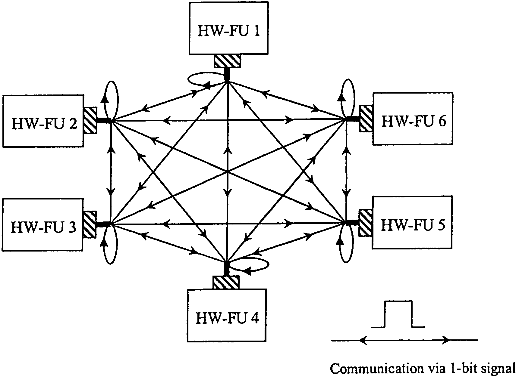
  • Decentralised fault-tolerant clock pulse generation in VLSI chips
  • Decentralised fault-tolerant clock pulse generation in VLSI chips
  • Decentralised fault-tolerant clock pulse generation in VLSI chips

Examples


Embodiment Construction

[0076]Based on the considerations discussed previously concerning the prior art technology, the virtually asynchronous or the GALS approach would have been very attractive if it had been possible to find a conceptually elegant solution to the problem with asynchronous communication between the synchronous islands. Thus, in addition, one should assume a structure consisting of locally synchronized functional units (modules) on one chip, these not being phase-synchronized to each other, but are frequency-synchronized to each other. Frequency synchronization in this context is concerned with matching the frequency of two or more clock pulse signals. Here, in contrast to phase synchronization, the period of time involved is larger. It is absolutely permissible that substantial phase shifts occur between the clock pulses during the interim period; however, what is decisive is that the number of phase changes in each time period under consideration may differ by not more than one a consta...


PUM


Abstract

The invention relates to a method for distributed, fault-tolerant clock pulse generation in hardware systems, wherein the system clock pulse is generated in distribution by a plurality of intercommunicating fault-tolerant clock pulse synchronization algorithms (TS-Algs), in which an arbitrary number of such TS-Algs exchange information between one another via a user-defined and permanent network (TS-Net) of clock pulse signals, susceptible to transient faults, and each TS-Alg is assigned to one or more functional units (Fu1, Fu2, . . . ), whose local clock pulses are generated by it, and further all local clock pulses are synchronized with respect to frequency in an assured manner, and a specified number of transient and / or permanent faults may occur in the TS-Algs or in the TS-Net, without adversely affecting the clock pulse generation and / or the synchronization accuracy, and the system clock pulse automatically achieves the maximum possible frequency. The invention further relates to such a hardware system.

Description

[0001]The future development of digital VLSI chips is characterized by constantly increasing integration density, complexity and clock frequency. This, however, increases the difficulty of providing, in all of the functional units (Fu), the synchronous clock pulses demanded by the synchronous design paradigm:[0002]Signals require a complete clock pulse cycle (and more) in order to address all functional units on the chip.[0003]There are demands for increasingly expensive procedures for skew optimization of the clock tree.[0004]Clock trees and buffers consume a large amount of power and surface area and are the cause of significant power supply problems and interference radiation.[0005]The maximum clock pulse frequency can only be determined on a place-&-route basis (and must be selected conservatively).[0006]Added to this is the fact that the clock pulse signal is a classical single point of failure:[0007]External quartz crystals are expensive, big and mechanically sensitive.[0008]E...

Claims


Application Information

Patent Timeline
Patent Type & Authority Patents(United States)
IPC IPC(8): G06F1/04
CPCG06F1/04G06F11/1604
Inventor SCHMID, ULRICHSTEININGER, ANDREAS
Owner VIENNA UNIVERSITY OF TECHNOLOGY
Learn More