Switched capacitor circuit with inverting amplifier and offset unit

a technology of inverter amplifier and capacitor, applied in the field of switching capacitor circuits, can solve the problems of high error and high power consumption of ota, and achieve the effect of reducing the area of the integrated circuit and reducing power consumption

Active Publication Date: 2010-09-21
SAMSUNG ELECTRONICS CO LTD +1
View PDF15 Cites 80 Cited by
  • Summary
  • Abstract
  • Description
  • Claims
  • Application Information

AI Technical Summary

Benefits of technology

[0013]Accordingly, the present invention uses an inverter for forming a switched capacitor circuit for reduced power consumption and reduced integrated circuit area.
[0027]In this manner, the switched capacitor circuit uses a simple single-ended inverter for forming a feedback loop for reduced power consumption and reduced integrated circuit area.

Problems solved by technology

In addition, a switched capacitor circuit uses a capacitor instead of a resistor that may result in higher error, for improving accuracy when a single integrated circuit chip is fabricated during a CMOS process.
However, the OTA consumes much power and occupies a large circuit area in the switched capacitor circuit 10.

Method used


Image

  • Switched capacitor circuit with inverting amplifier and offset unit
  • Switched capacitor circuit with inverting amplifier and offset unit
  • Switched capacitor circuit with inverting amplifier and offset unit

Examples


Embodiment Construction

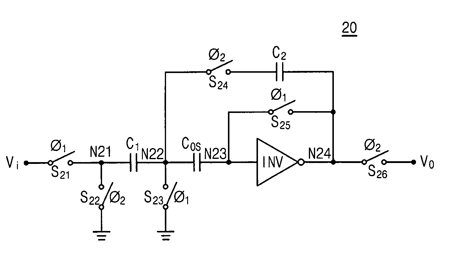
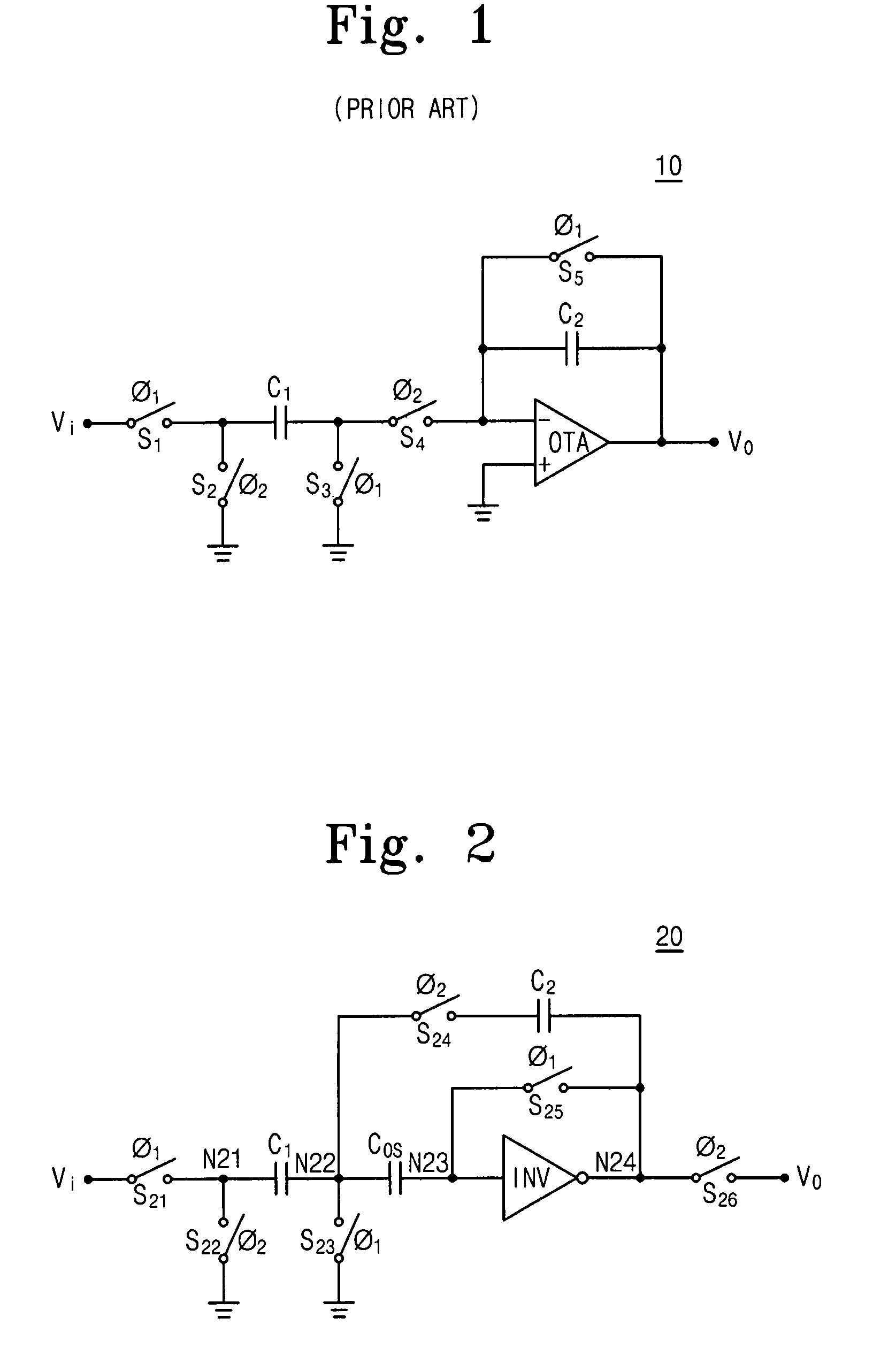
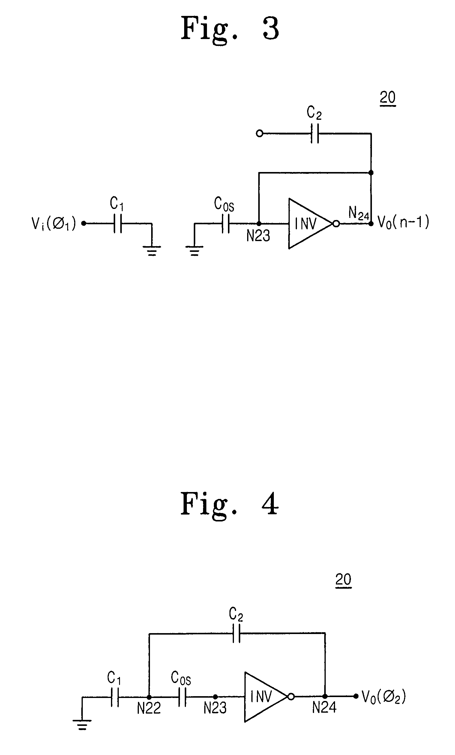
[0040]FIG. 2 shows a switched capacitor circuit 20 for implementing an integrator according to an embodiment of the present invention. Referring to FIG. 2, the switched capacitor circuit 20 includes an inverter INV, and first, second, third, fourth, fifth, and sixth switches S21, S22, S23, S24, S25, and S26, respectively. The switched capacitor circuit 20 also includes a sampling capacitor C1, an offset capacitor Cos, and a feedback capacitor C2.

[0041]The inverter INV is single-ended with a single input and a single output according to an embodiment of the present invention. Such an inverter has a simpler circuitry than the OTA of the prior art such that the switched capacitor circuit 20 consumes less power and occupies less integrated circuit area. The inverter INV is a typical inverter having a gain of about −1 in one embodiment of the present invention. Alternatively, the inverter INV is an inverting amplifier providing a negative gain with a magnitude of the gain being greater t...


PUM


Abstract

A switched capacitor circuit includes an amplifier, a charging unit, an offset unit, and an integrating unit. The charging unit is coupled between an input node and a first node, and is for accumulating charge corresponding to an input signal during a sampling mode. The offset unit is coupled between the first node and an input of the amplifier, and is for maintaining the first node to be a virtual ground during an integrating mode. The integrating unit is coupled between the first node and an output of the amplifier, and is for receiving charge from the charging unit during the integrating mode.

Description

BACKGROUND OF THE INVENTION[0001]This application claims priority under 35 USC §119 to Korean Patent Application No. 2006-115386 filed on Nov. 21, 2006 in the Korean Intellectual Property Office, the disclosure of which is incorporated herein in its entirety by reference.[0002]1. Field of the Invention[0003]The present invention relates generally to switched capacitor circuits, and more particularly, to a switched capacitor circuit implemented with a single ended inverter and an offset unit for rendering a node as virtual ground.[0004]2. Background of the Invention[0005]A switched capacitor circuit is generally a type of filter that is comprised of capacitors and switches without any inductor or resistor. A switched capacitor circuit is amenable to be fabricated with the complementary metal-oxide-semiconductor (CMOS) process. A switched capacitor circuit is easily integrated with the CMOS process in a single chip without resistors and is amenable for decreased power consumption.[000...

Claims


Application Information

Patent Timeline
Patent Type & Authority Patents(United States)
IPC IPC(8): G06G7/184H03M3/02
CPCH03H19/004H03M3/356H03M3/43H03M3/456H03F1/32
Inventor CHAE, YOUNGCHEOLHAN, GUNHEEHAM, SEOG-HEON
Owner SAMSUNG ELECTRONICS CO LTD
Why Eureka
Try Eureka