Current-leveling electroplating/electropolishing electrode

a current leveling and electroplating technology, applied in the field of electroplating/electropolishing processes, can solve the problems of degrading device failure or burn-in, overpolishing burden during subsequent cmp processing, etc., to achieve uniform current distribution, improve em or sm reliability, and uniform thickness

Inactive Publication Date: 2010-09-28
TAIWAN SEMICON MFG CO LTD
View PDF7 Cites 6 Cited by
  • Summary
  • Abstract
  • Description
  • Claims
  • Application Information

AI Technical Summary

Benefits of technology

[0016]The present invention is generally directed to a novel current-leveling electroplating / electropolishing electrode which facilitates uniform current distribution during an ECP or electrochemical polishing process to deposit or electropolish a metal layer having a substantially uniform thickness on a substrate. The current-leveling electrode includes a base electrode and one or multiple sub-electrodes which, depending on the desired electroplating or electropolishing profile to be formed on a substrate, can be attached to the base electrode to impart a stepped, convex or non-planar configuration to the electrode. Accordingly, during an electroplating or electropolishing process, the stepped profile of the electrode establishes higher current densities between the electrode and the center portion of a substrate as compared to the current density between the electrode and the edge of the substrate. This results in electroplating or electropolishing of a metal layer having a substantially uniform thickness on the substrate, thereby improving the yield and reliability of devices fabricated on a wafer. Furthermore, the flexible structure of the current-leveling electrode facilitates improved process throughput by widening the process window for copper electroplating.

Problems solved by technology

These voids or open circuits may cause device failure or burn-in.
This, in turn, leads to overpolishing burden during subsequent CMP processing.
Furthermore, non-uniform grain sizes between the wafer edges and center as a result of electroplating may degrade the EM or SM reliability.
A common drawback of this method, however, is that EBR processes eliminate usable die areas on the wafer (about 2-5 mm for 8″ wafers).
However, these methods have shown limited effectiveness.
However, like electroplating techniques, copper electropolishing techniques result in the formation of metal layers having a non-uniform thickness caused by non-uniform current distribution in the electrochemical plating tank.

Method used


Image

  • Current-leveling electroplating/electropolishing electrode
  • Current-leveling electroplating/electropolishing electrode
  • Current-leveling electroplating/electropolishing electrode

Examples


Embodiment Construction

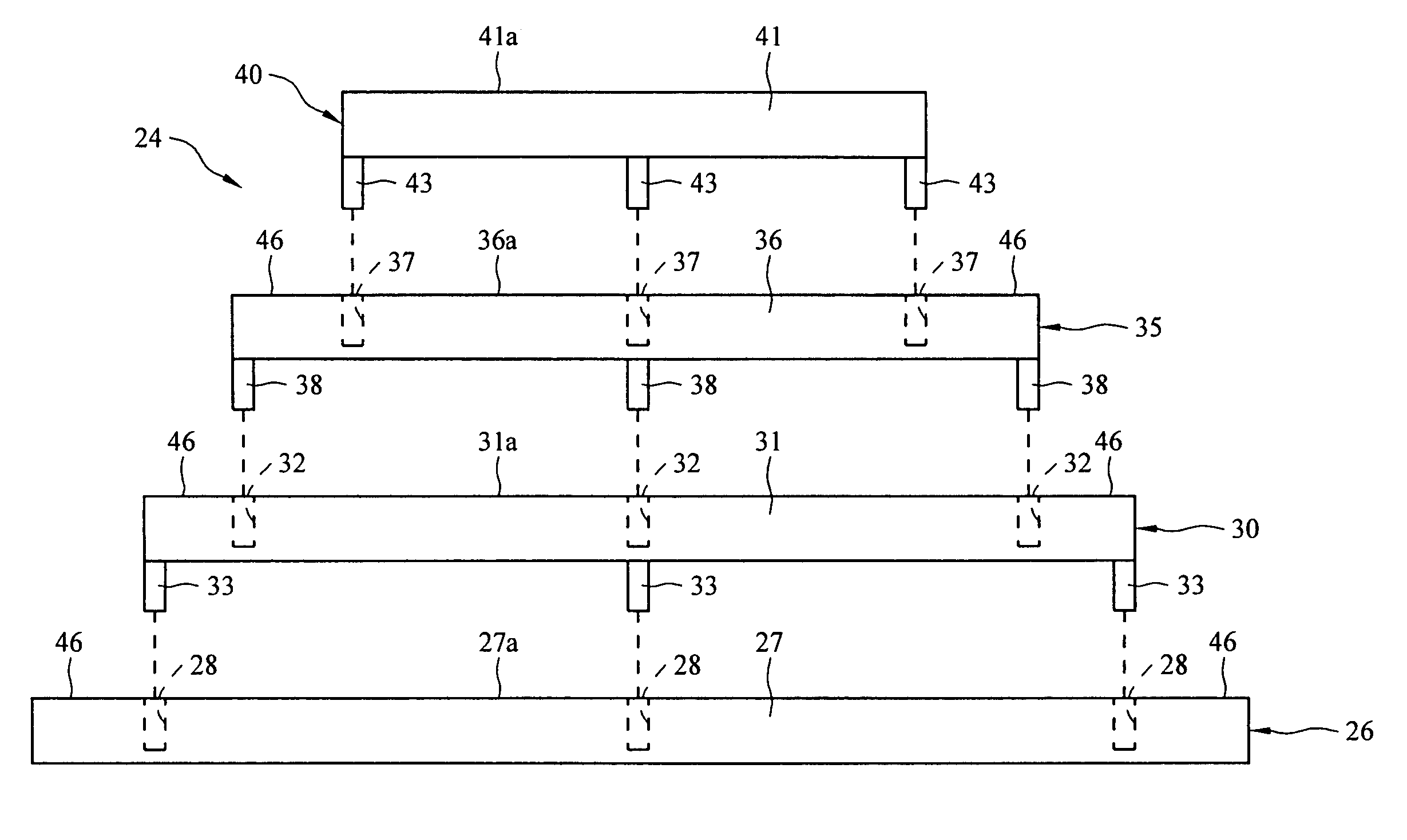
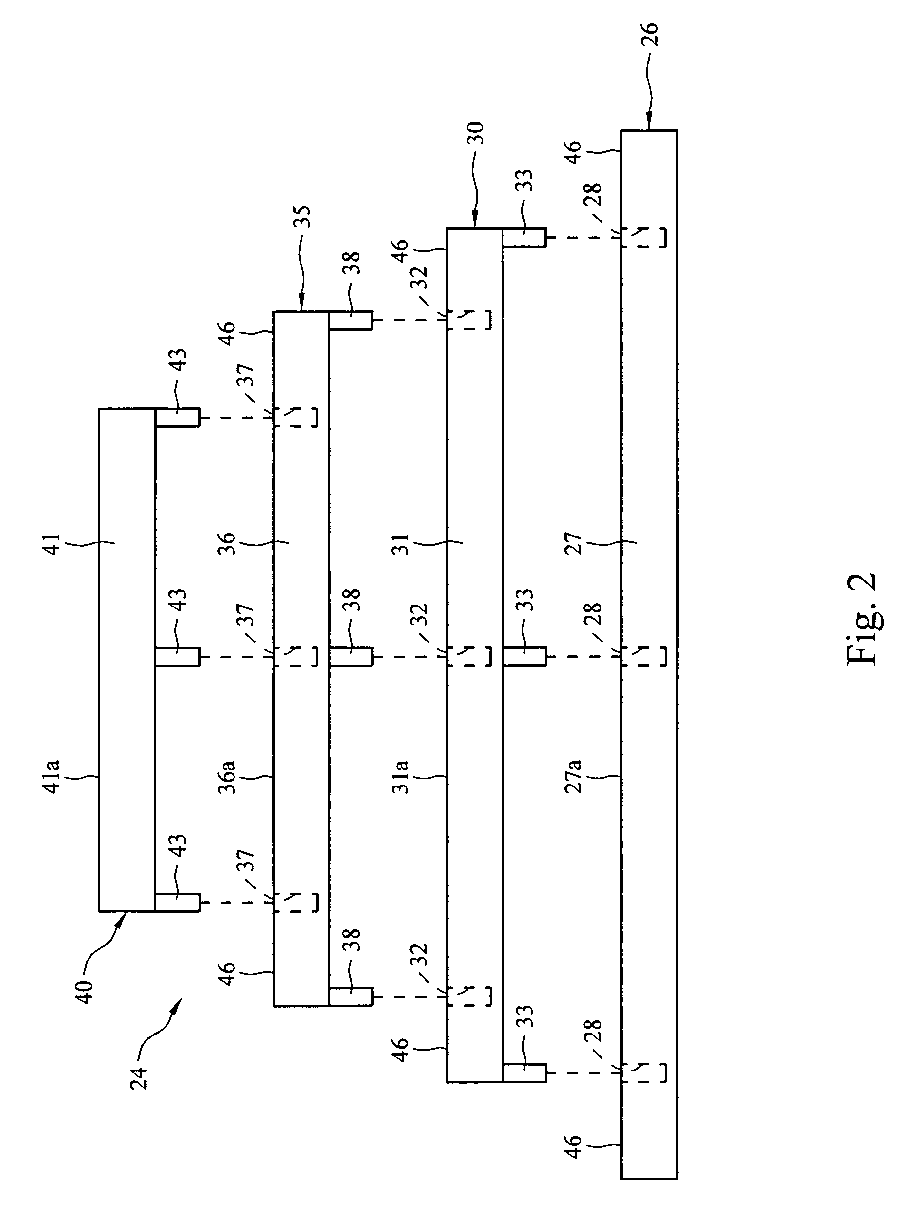
[0022]The present invention contemplates a novel current-leveling electroplating / electropolishing electrode which has a flexible geometry to facilitate uniform current distribution between an anode and a cathode in an electroplating or electropolishing process. The current-leveling electrode includes a base electrode and multiple sub-electrodes a selected number of which can be attached to the base electrode to impart a stepped, convex or non-planar configuration to the electrode, depending on the desired electroplating or electropolishing profile to be formed on a substrate. Accordingly, during an electroplating or electropolishing process, the stepped profile of the electrode establishes higher current densities between the electrode and the center portion of a substrate as compared to the current density between the electrode and the edge portion of the substrate. Consequently, in an electroplating process, a metal layer having a substantially uniform thickness is deposited on th...


PUM

PropertyMeasurementUnit
voltage potentialaaaaaaaaaa
widthaaaaaaaaaa
solubleaaaaaaaaaa

Abstract

A current-leveling electrode for improving electroplating and electrochemical polishing uniformity in the electrochemical plating or electropolishing of metals on a substrate is disclosed. The current-leveling electrode includes a base electrode and at least one sub-electrode carried by the base electrode. The at least one sub-electrode has a width which is less than a width of the base electrode to impart a generally tapered, stepped or convex configuration to the current-leveling electrode.

Description

FIELD OF THE INVENTION[0001]The present invention relates to electrochemical plating (ECP) / electropolishing processes used to deposit / polish metal layers on semiconductor wafer substrates in the fabrication of semiconductor integrated circuits. More particularly, the present invention relates to a current-leveling electrode which includes a base electrode and one or multiple sub-electrodes which can be selectively added to the base electrode to improve uniformity in the electroplating or electropolishing of metals on a substrate.BACKGROUND OF THE INVENTION[0002]In the fabrication of semiconductor integrated circuits, metal conductor lines are used to interconnect the multiple components in device circuits on a semiconductor wafer. A general process used in the deposition of metal conductor line patterns on semiconductor wafers includes deposition of a conducting layer on the silicon wafer substrate; formation of a photoresist or other mask such as titanium oxide or silicon oxide, in...

Claims


Application Information

Patent Timeline
Patent Type & Authority Patents(United States)
IPC IPC(8): C25D17/14C25D17/12
CPCC25D17/12H01L21/2885C25D17/001Y10T29/49208Y10T29/53204
Inventor CHANG, SHIH-CHIEHWANG, YING-LANGCHEN, KEI-WEILIN, SHIH-HOCHEN, CHUN-CHANG
Owner TAIWAN SEMICON MFG CO LTD
Why Eureka
Try Eureka