Wideband planar transformer

a planar transformer and wideband technology, applied in fixed transformers, magnets, magnetic bodies, etc., can solve the problems of poor return loss and insertion loss of prior art planar transformers over a wide frequency range, limited use of low speed or narrow band applications, and insufficient application of prior art approaches. , to achieve the effect of accurately designed and adjusted, reducing the permeability of the core, and reducing the reflected energy and loss

Active Publication Date: 2010-10-26
PLANARMAG
View PDF62 Cites 35 Cited by
  • Summary
  • Abstract
  • Description
  • Claims
  • Application Information

AI Technical Summary

Benefits of technology

[0007]The current invention provides a method of arranging windings to minimize reflected energy and loss and fabrication techniques for the invented windings of a wideband planar transformer. According to one embodiment, the method provides for the inter-winding of the primary and the secondary turns so that the winding capacitance can be specifically designed for coupling up to GHz even when the permeability of the core significantly drops. A primary turn is inter-wound with an adjacent secondary turn with a spacing that can be specifically designed and controlled with micro-fabrication techniques. The primary and secondary turns are adjacent at the top, bottom and the two vertical sides. The adjacent primary and secondary turns wrap around the toroid from top to bottom to provide necessary coupling at GHz frequency. The number of turns, spacing between the primary and secondary turns and width of the each turns can all be accurately designed and adjusted to control the parasitic effects. The coupling between the primary and secondary turns can be adjusted accordingly to achieve the lowest reflected energy and loss. The center taps are an electrode connected to the middle of the primary and the secondary turns.
[0008]One aspect of the above embodiment, the number of the primary and secondary turns is an even number. On the primary side, one turn is open to provide the differential input. This leaves an odd number of turns on the primary side. The center tap is connected in the middle of the remaining odd primary turns. Hence, the number of turns on either side of the center tap is even or balanced. The same center tap configuration and turns are used on the secondary side. This arrangement of the turns and the center taps significantly minimizes the conversion of the differential mode to common mode signals to avoid EMI. According to one embodiment, the method includes providing a bottom mold that has a pattern of hole pairs disposed in a planar base of the bottom mold. Conductive elements are inserted to the holes, where the conductive elements are disposed vertically from the planar base, and a bottom portion of the conductive elements are held by the bottom mold. The method further includes providing a first top mold that is disposed on the bottom mold forming a first mold pair, where the first top mold has conductive element receiving features and a displacement feature disposed between the conductive element receiving features, such that a middle portion of the conductive elements spans between the first top mold and the bottom mold. A dielectric material is deposited to the first mold pair that envelopes the middle portion of the conductive elements and further envelopes the displacement feature. The first top mold is removed, where a vacancy is then revealed by removing the displacement feature. A ferrite element is deposited to the vacancy. A second top mold is provided to the bottom mold, where the second top mold and the bottom mold define a second mold pair, and the second top mold spans the bottom mold. The dielectric material is deposited to the second mold pair to create a molded assembly, where the dielectric material envelopes a top portion of the conductive element and envelopes the ferrite element. The molded assembly is removed from the second mold pair, where the molded assembly has a top surface and a bottom surface. The top surface and the bottom surface are prepared for receiving a pattern of conductive coatings, where the preparation includes removing the top and bottom conductive element portions such that the top and bottom surfaces have the dielectric material and planed ends of the conductive element middle portion. The conductive coating is applied, where the coating is disposed to connect the middle portion conductive element ends according to a conductive pattern, wherein the conductive pattern defines a primary coil and a secondary coil of the wideband planar transformer.

Problems solved by technology

Both of these methods have severe limitations, which restrict their use to low speed or narrow band applications.
In the case of planar transformer designs prior art approaches fail to adequately address a method of arranging the windings to control leakage inductance and winding capacitance and its associated fabrication.
As result, prior art planar transformers have poor return loss and insertion loss over a wide frequency range and are not functional and usable in many communication standards today.
Transformers based on this prior art consistently fail to meet the technical requirements for data communications and are restricted to relatively low speed applications such as switching power supply systems.
Integration of magnetic materials onto Si tends to be difficult.
Furthermore, integrated transformers suffer parasitic eddy currents generated by the magnetic fields in the silicon and have limited high frequency performance.
As a result, integrated transformers typically have narrow band-pass characteristics and are only good for narrow frequency balun applications commonly found in wireless applications such as cellular phones.
These center taps make it very difficult to achieve wide bandwidth performance.
The increase in the number of turns induces significant leakage inductance and winding capacitance that degrade the transfer of energy and reflect significant energy.

Method used


Image

  • Wideband planar transformer
  • Wideband planar transformer
  • Wideband planar transformer

Examples


Embodiment Construction

[0024]Although the following detailed description contains many specifics for the purposes of illustration, anyone of ordinary skill in the art will readily appreciate that many variations and alterations to the following exemplary details are within the scope of the invention. Accordingly, the following preferred embodiment of the invention is set forth without any loss of generality to, and without imposing limitations upon, the claimed invention.

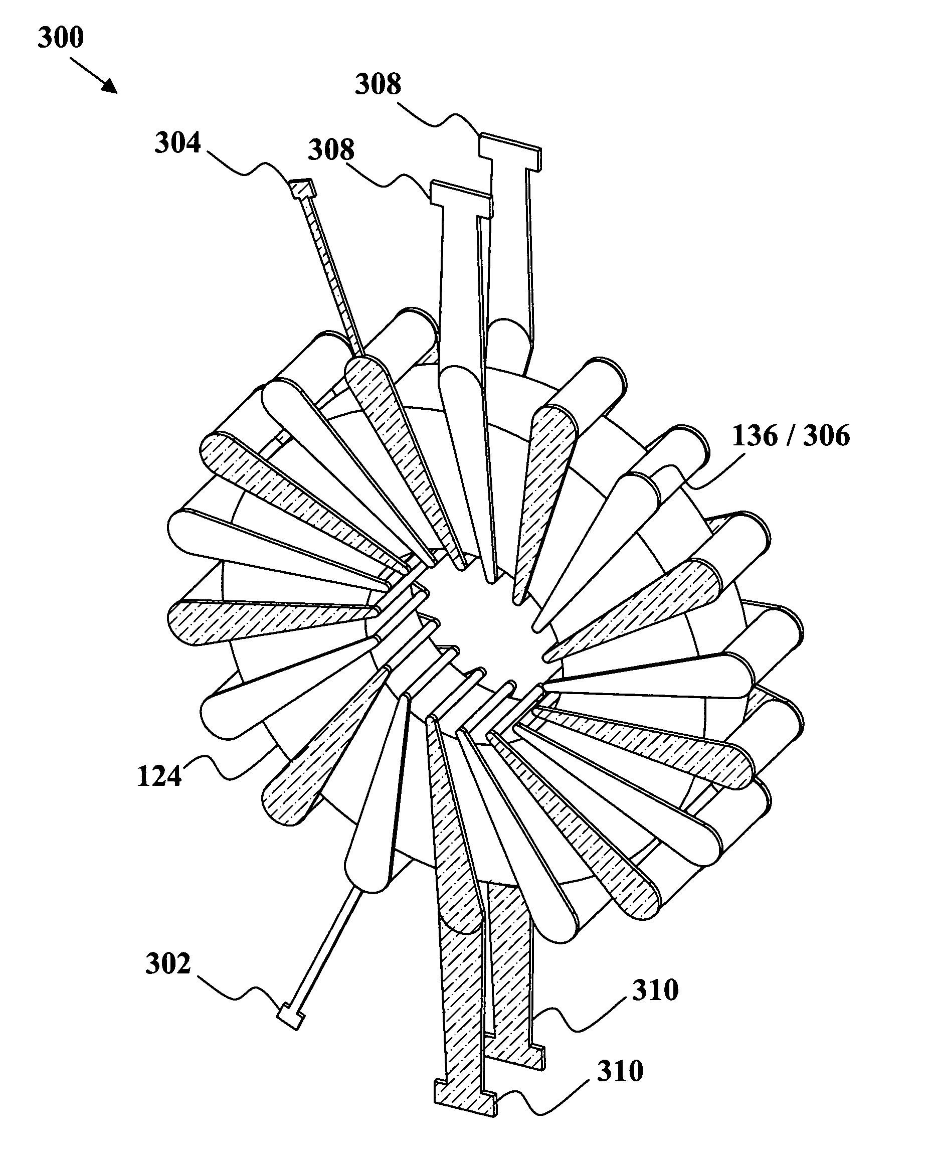
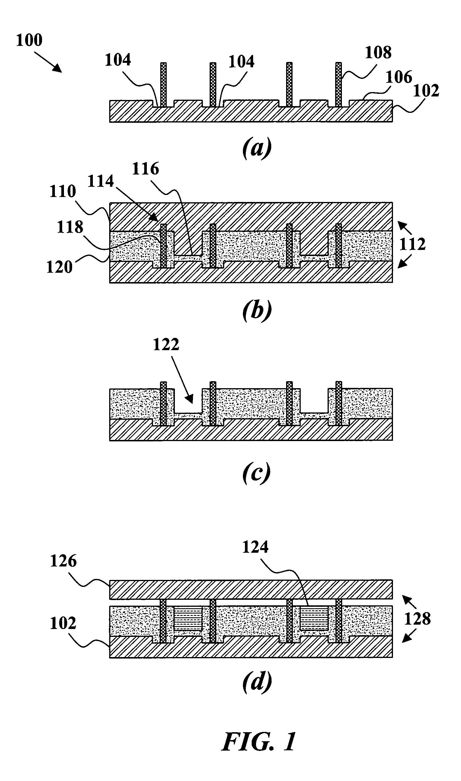
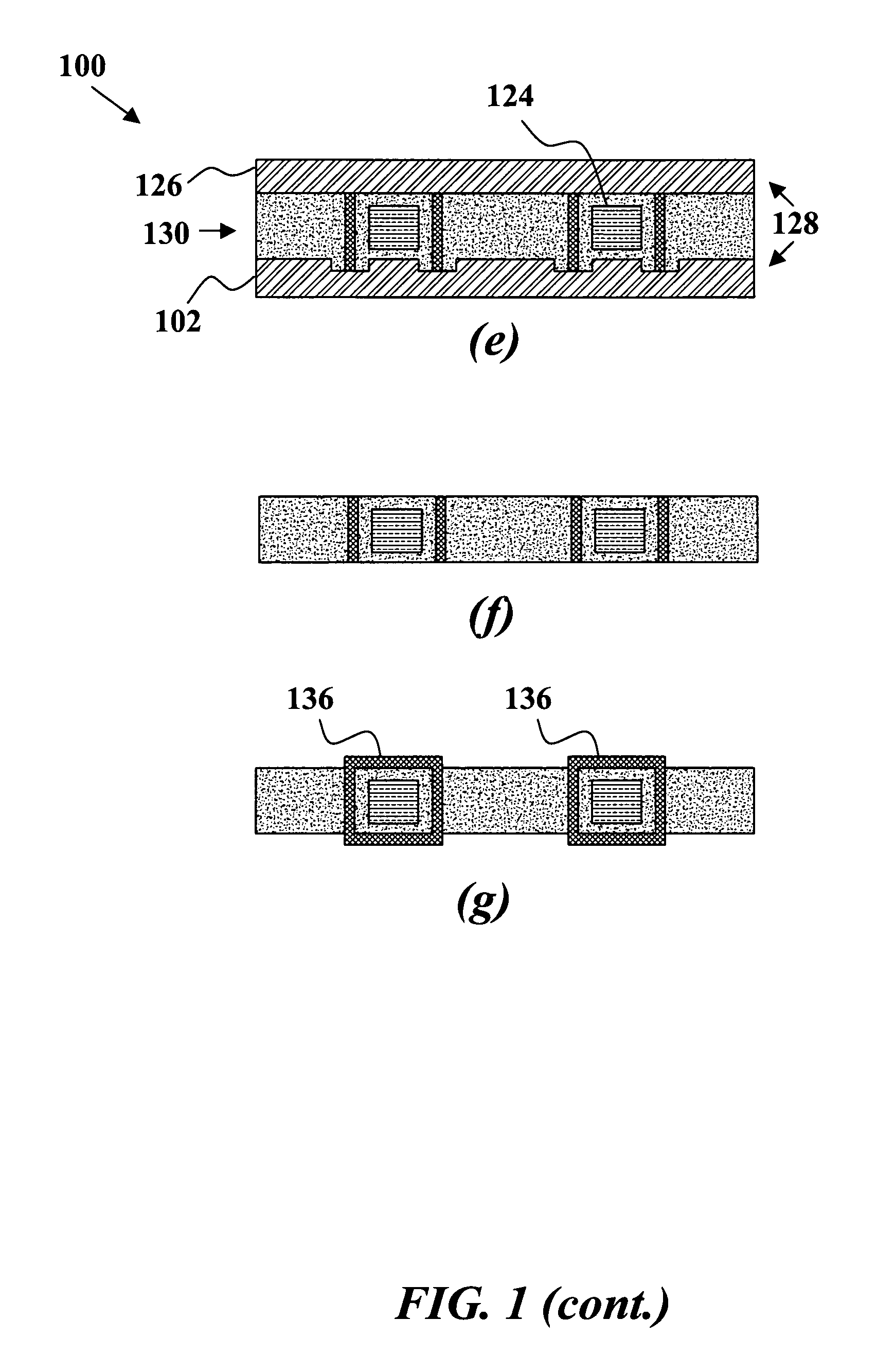
[0025]Creating a wideband planar transformer according to the current invention requires the use of several different concepts together in one design. The current method uses physical design and layout aspects that enable the conductors to be inter-wound around the ferrite material and adjacent conductors. In wideband applications, conductor spacing is critical as the frequency increases, where at low frequencies the ferrite material will provide sufficient coupling but at frequencies above several hundred megahertz the ferrite permeabili...


PUM

PropertyMeasurementUnit
voltageaaaaaaaaaa
frequenciesaaaaaaaaaa
impedanceaaaaaaaaaa

Abstract

A method of arranging and fabricating parallel primary and secondary coils of a wideband planar transformer is provided. The spacing and width of the coils are disposed to extend the bandwidth from DC to GHz and allow for high frequency coupling when the core permeability dramatically drops and achieves low reflected energy and low loss over a wide bandwidth. A bottom mold having a pattern of hole-pairs with conductive elements inserted vertically couples to a top mold such that a middle portion of the conductive elements spans between the top and bottom molds. Dielectric material envelopes the middle portion and a displacement feature of the mold creates a vacancy. A ferrite element is deposited to the vacancy. A second top mold spans the bottom mold and dielectric material is deposited to create a molded assembly. A deposited patterned conductive coating connects the element ends to define the transformer coils.

Description

CROSS-REFERENCE TO RELATED APPLICATIONS[0001]This application is cross-referenced to and claims the benefit from U.S. Provisional Patent Application 60 / 880,208 filed Jan. 11, 2007, which is hereby incorporated by reference.FIELD OF THE INVENTION[0002]The invention relates generally to DC to multi-GHz's bandwidth magnetic-winding communications circuitry. More particularly, the invention relates to a method of arranging micro-fabricated windings with molded ferrite cores to specifically control leakage inductance and winding capacitance to achieve GHz performance and electrical consistency.BACKGROUND[0003]There has been much attention directed to planar or integrated transformers using PCB boards or semiconductors over the last ten years. Planar transformers are manufactured using a combination of embedded or attached ferrite materials and PCB techniques to improve the winding coupling. In the case of semiconductors, attempts are made to integrate the entire inductor or transformer s...

Claims


Application Information

Patent Timeline
Patent Type & Authority Patents(United States)
IPC IPC(8): H01F27/28H01F27/29H01F5/00H01F29/00
CPCH01F19/04H01F41/046H01F17/0033Y10T29/4902H01F2027/2814H01F30/16
Inventor HARRISON, WILLIAM LEEMCCONNELL, STEPHEN M.PHAM, ANH-VU
Owner PLANARMAG
Why Eureka
Try Eureka