On-chip packet interface processor encapsulating memory access from main processor to external system memory in serial packet switched protocol

a serial packet switching and processor technology, applied in the field of communication architectures, can solve the problems of limited operation bandwidth, difficult implementation, and limited local system buses that can operate as parallel bus interconnections at speeds that match the processor speed, and achieve the effect of further reducing the overhead of ethernet protocol

Inactive Publication Date: 2010-10-26
KIRITIN INC
View PDF4 Cites 21 Cited by
  • Summary
  • Abstract
  • Description
  • Claims
  • Application Information

AI Technical Summary

Benefits of technology

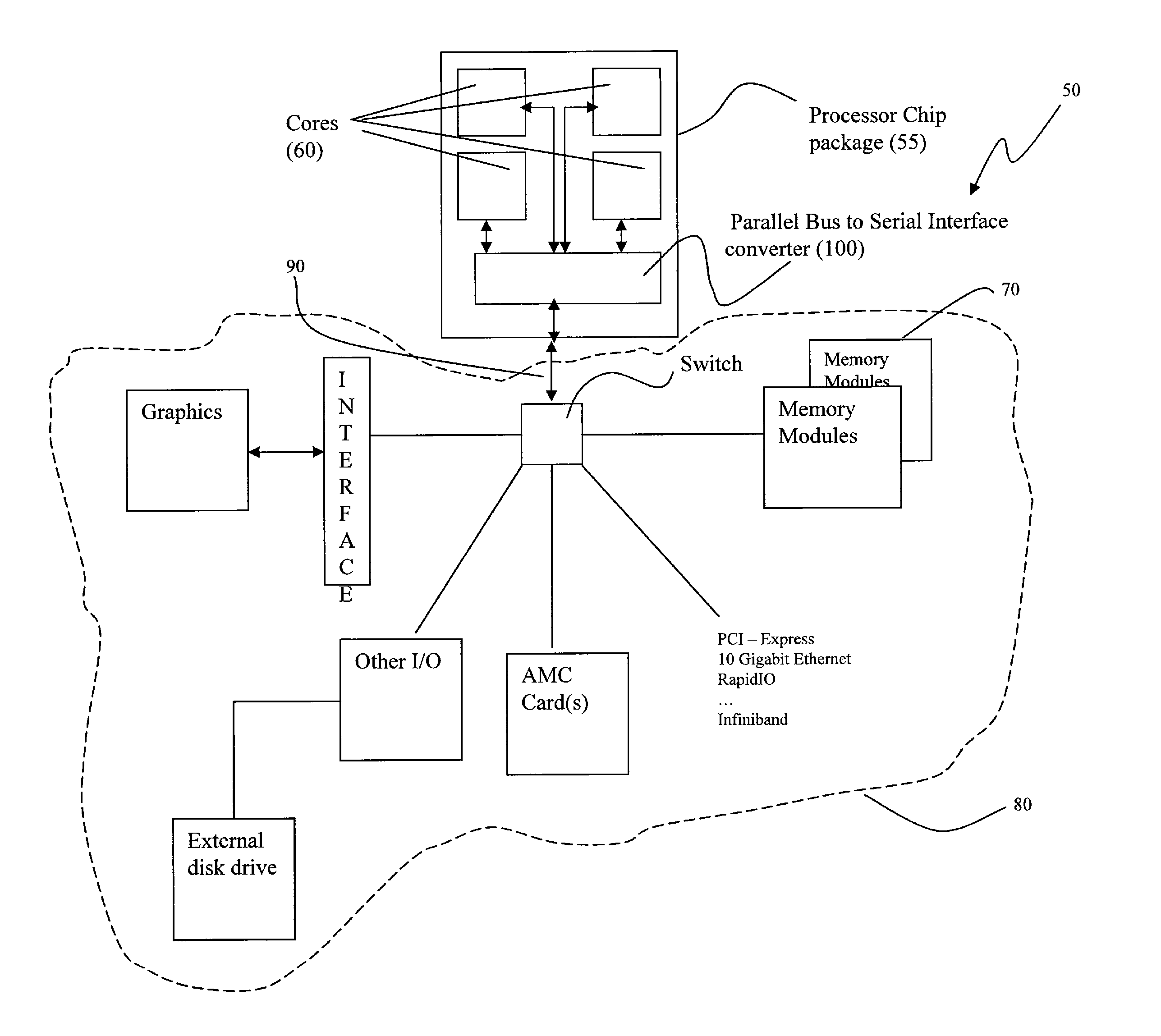
[0021]In an exemplary embodiment, the packet processor is implemented as a on the fly programmable bit stream protocol processor integrated as part of the chip. In one embodiment, a processor chip with cache can connect to a system or main memory chipset via a bit stream protocol processor incorporated as part of the microprocessor chip. In one embodiment the processor serial interface can be a 10 Giga bit Ethernet interface. In these embodiments, the protocol processor encapsulates the memory address and control information like Read, Write, number of successive bytes etc, as an Ethernet packet for communication among the processor(s) and memory chips that are located on the same chip, or on the motherboard, or alternatively on different circuit cards. In one embodiment, the communication overhead of the Ethernet protocol is further reduced by using an enhanced Ethernet protocol with shortened data frames within a constrained neighborhood, and / or by utilizing a bit stream switch where direct connection paths can be established between elements that comprise the computing or communication architecture.

Problems solved by technology

This architecture requires instructions and data be fetched sequentially introducing a limitation in operation bandwidth which is often termed the “Von Neuman Bottleneck”.
Processors and memories that can operate at upwards of 3 GHz clock are known, but local system buses that can operate as a parallel bus interconnection at speeds that match the processor speeds are very rare as such high speed buses are difficult to implement.
One of the challenges in attempting to increase the speed of I / O buses, such as the PCI bus and PCI Extended (PCI X) bus, is that a parallel bus arrangement is prone to problems of clock skew between data flowing in the separate parallel data paths that may, for example, differ from each other by a very small path length.
Clock recovery and data reconstruction prove to be increasingly problematic and unreliable as path lengths, data transfer speeds and / or the number of parallel paths are increased.
Additionally, parallel buses take up considerable circuit board real estate.
Unfortunately, this is a proprietary solution that is incompatible with the general trend of migrating to the adoption of industry wide standards that encourage vendors to develop products which are interoperable with other vendors' solutions so as to reduce time and cost to market for new products.
The problem created by this divergence between processor speeds and memory access speeds is well known and has been referred to in the prior art as the memory gap or memory wall problem.
The memory gap problem is further compounded by the need to address a large memory capacity.
Unfortunately, this proposal was not widely adopted.
While the speeds of a serial I / O protocol theoretically could approach the speeds needed for the processor / memory interface, the communication overhead associated with serial I / O protocols has curtailed any serious attempts to consider using serial I / O protocols as a basis for a processor / memory interface.
The larger packet and address sizes results in an increased communication overhead penalty.
The processor / memory interface conventionally has required the ability to transfer data between the processor and memory for a single address location, a requirement for which the overhead of I / O transfers and protocols has been seen as massive overkill.
In addition, there are many more transmission blocking and memory contention concerns that need to be addressed for I / O communications than for processor-to-memory interfaces.
These issues have generally discouraged the adoption of serial I / O protocols for communications between processors and memory even as such serial I / O protocols are being used in the smaller physical dimensions of a circuit board or a computer or communication rack or cabinet having multiple cards / blades interconnected by a backplane.
As processor speeds, memory speeds and network speeds continue to increase, and as the external I / O is increasingly capable of delivering data at rates exceeding gigabit speeds, the current architectures for arranging the subsystems within a computing and communication architecture are no longer efficient.

Method used


Image

  • On-chip packet interface processor encapsulating memory access from main processor to external system memory in serial packet switched protocol
  • On-chip packet interface processor encapsulating memory access from main processor to external system memory in serial packet switched protocol
  • On-chip packet interface processor encapsulating memory access from main processor to external system memory in serial packet switched protocol

Examples


Embodiment Construction

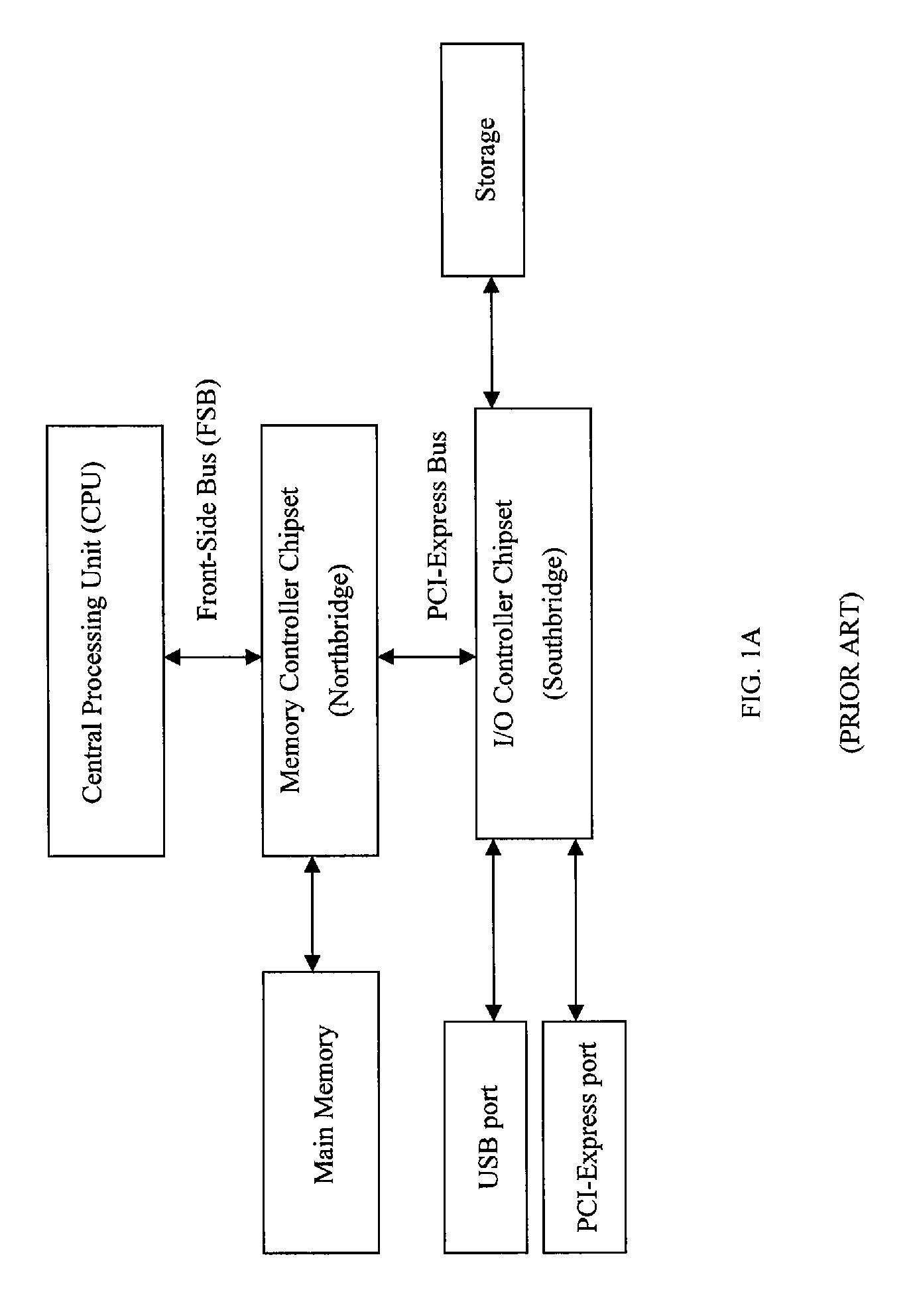
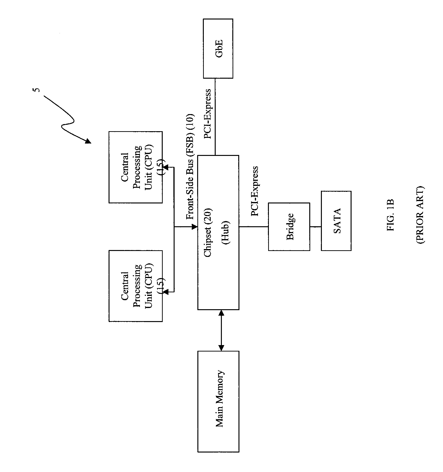
[0037]FIGS. 1A, 1B, 1C, 1D, and 1E illustrate various configurations of front side bus (alternately “Channel”) arrangements for prior art processor chipset architectures. In each of these configurations, a clocked bus interface 10 is used between the processor chip 15 and one or more support chips 20 for purposes of routing data and instructions among the various elements of the computer architecture 5.

[0038]Conventional architectures feature a channel, variously referred to as the Front Side Bus (“FSB”), the Processor Side Bus, the Memory Bus, the Data Bus, or the System Bus, over which the CPU communicates with, for example, a motherboard chipset such as the Northbridge and Southbridge controllers illustrated, for example, in FIG. 1D. The Northbridge 25 interconnects the CPU 15 to the RAM memory 30 via the FSB. The Northbridge also connects peripherals such as the graphics card 35 via high speed channels such as the AGP and the PCI Express. The Southbridge controller 40 handles I / ...


PUM


Abstract

A computing and communication chip architecture is provided wherein the interfaces of processor access to the memory chips are implemented as a high-speed packet switched serial interface as part of each chip. In one embodiment, the interface is accomplished through a gigabit Ethernet interface provided by protocol processor integrated as part of the chip. The protocol processor encapsulates the memory address and control information like Read, Write, number of successive bytes etc, as an Ethernet packet for communication among the processor and memory chips that are located on the same motherboard, or even on different circuit cards. In one embodiment, the communication over head of the Ethernet protocol is further reduced by using an enhanced Ethernet protocol with shortened data frames within a constrained neighborhood, and / or by utilizing a bit stream switch where direct connection paths can be established between elements that comprise the computing or communication architecture.

Description

PRIORITY CLAIM[0001]The present invention claims priority to U.S. Provisional Application Ser. No. 60 / 887,989, filed Feb. 2, 2007, entitled “Processor Chip Architecture Having Integrated High-Speed Packet Switched Serial Interface,” the disclosure of which is hereby incorporated by reference.RELATED APPLICATIONS[0002]The present invention is related to U.S. application Ser. No. 11 / 828,329, filed Jul. 25, 2007, entitled “Telecommunication and Computing Platforms with Serial Packet Switched Integrated Memory Access Technology,” and U.S. application Ser. No. 11 / 838,198, filed Aug. 13, 2007, entitled “Enhanced Ethernet Protocol for Shortened Data Frames Within a Constrained Neighborhood Based on Unique ID,” U.S. application Ser. No. 11 / 466,367, filed Aug. 23, 2006, entitled “Omni-Protocol Engine for Reconfigurable Bit-Stream Processing in High-Speed Networks,” the disclosures of each of which are hereby incorporated by reference.FIELD OF THE INVENTION[0003]The present invention relates ...

Claims


Application Information

Patent Timeline
Patent Type & Authority Patents(United States)
IPC IPC(8): G06F13/14
CPCG06F15/16H04L12/4625G06F13/382H04L12/56G06F13/4022G06F13/4282G06F13/14G06F13/20G06F13/40
Inventor SHARMA, VISWA
Owner KIRITIN INC
Why Eureka
Try Eureka