Fluorescent material with semiconductor nanoparticles dispersed in glass matrix at high concentration and method for manufacturing such fluorescent material

a technology of glass matrix and semiconductor nanoparticles, which is applied in the field of fluorescent materials, can solve the problems of unstable semiconductor nanoparticles produced by the aqueous solution method, low light, heat, chemical resistance of polymers used as a matrix, and unsuitable industrial applications, and achieves high fluorescence quantum yield, high concentration, and high brightness

Inactive Publication Date: 2010-11-02
NAT INST OF ADVANCED IND SCI & TECH
View PDF7 Cites 5 Cited by
  • Summary
  • Abstract
  • Description
  • Claims
  • Application Information

AI Technical Summary

Benefits of technology

[0129]In the fluorescent material of the present invention, semiconductor nanoparticles exist in a stable condition in a glass matrix, and the semiconductor nanoparticles maintain a high fluorescence quantum yield and a high concentration. Therefore, the fluorescent material of the present invention is a thin-film fluorescent material whose level of brightness is higher than that of any other heretofore-known fluorescent materials.
[0130]The fluorescent material of the present invention having the above-described outstanding properties can provide optical devices, such as display devices and lighting systems with a high level of brightness in place of conventional fluorescent materials.

Problems solved by technology

However, the semiconductor nanoparticles produced by the aqueous solution method are unstable while still in the aqueous solution state, and are not suitable for industrial applications.
However, polymers used as a matrix have low levels of light, heat, and chemical resistance, as well as other properties, and gradually permit the passage of water and oxygen.
The resulting drawback is a gradual degradation of the fixed nanoparticles.
However, a fluorescent material produced by the simple mixing mentioned above does not always reach the required high brightness level.
However, in the known literature described above, an organic matrix is used, and the wavelength of fluorescence is sharply shifted to blue after nanoparticles are put into the matrix compared to the previous state, and moreover, the fluorescence has a considerable tail towards red due to defects on the surface of the nanoparticles in many cases.
In addition, an organic matrix is adopted, which causes problems such as low light, heat, and chemical resistance, moisture permeability, gas permeability and the like.
Moreover, the fixed semiconductor nanoparticles deteriorate gradually, causing poor long-term stability.
However, under the present circumstances, a satisfactory thin-film fluorescent material cannot be provided.Patent Document 1: WO 2004-000971, pamphletPatent Document 2: WO 2004-065296, pamphletNon-Patent Document 1: Gao, et al., Journal of Physical Chemistry, B, vol.

Method used


Image

  • Fluorescent material with semiconductor nanoparticles dispersed in glass matrix at high concentration and method for manufacturing such fluorescent material
  • Fluorescent material with semiconductor nanoparticles dispersed in glass matrix at high concentration and method for manufacturing such fluorescent material
  • Fluorescent material with semiconductor nanoparticles dispersed in glass matrix at high concentration and method for manufacturing such fluorescent material

Examples


example 1

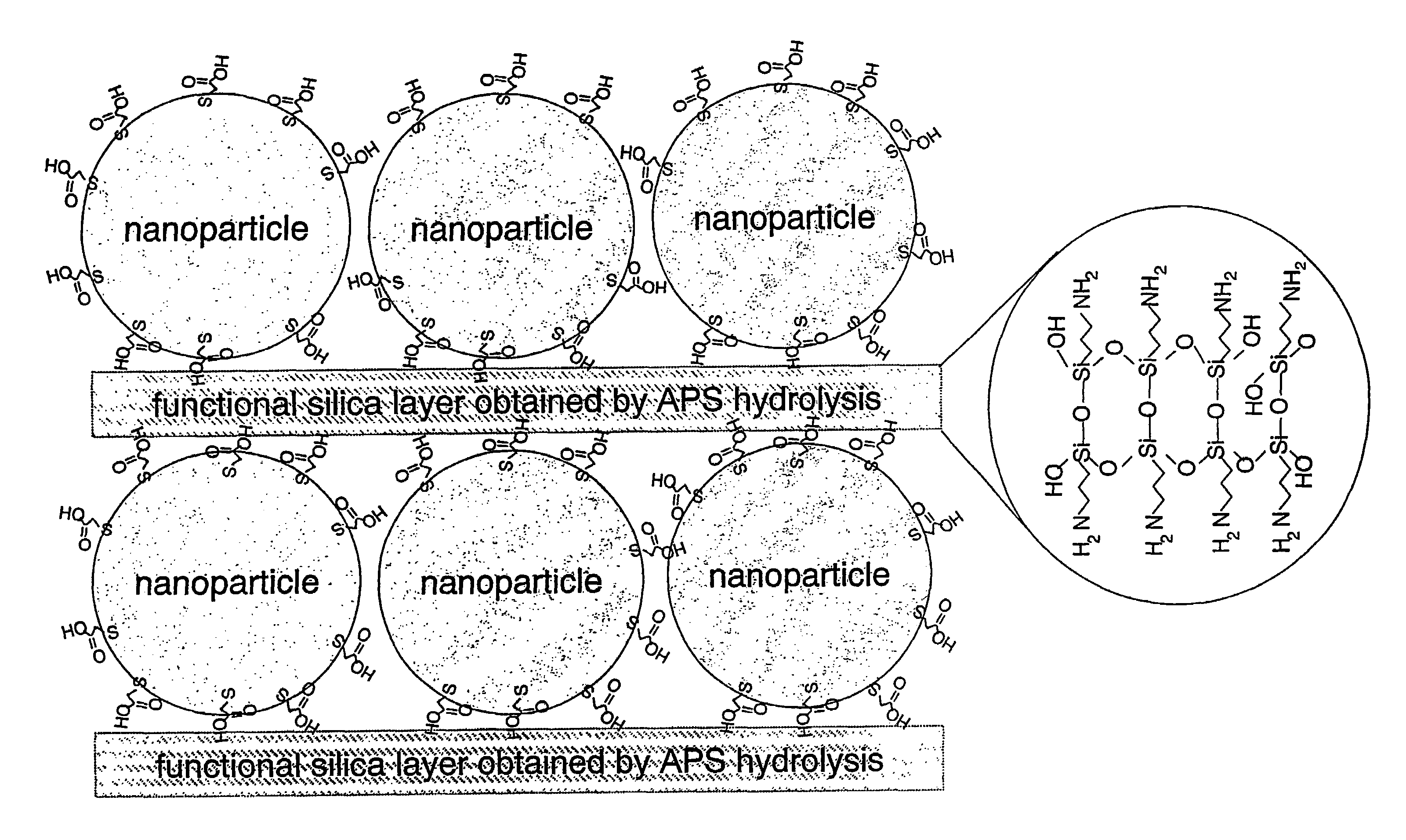
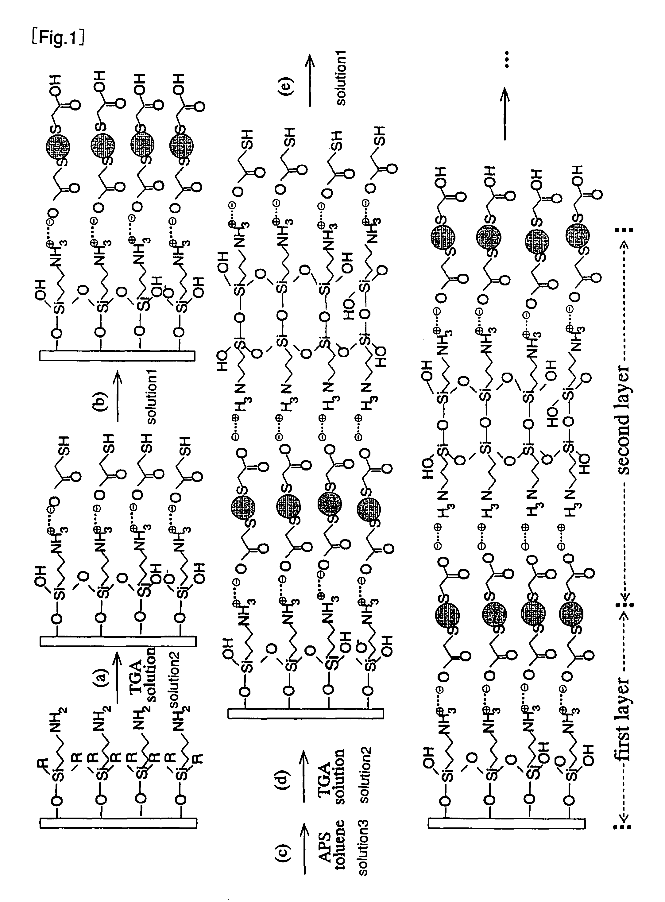
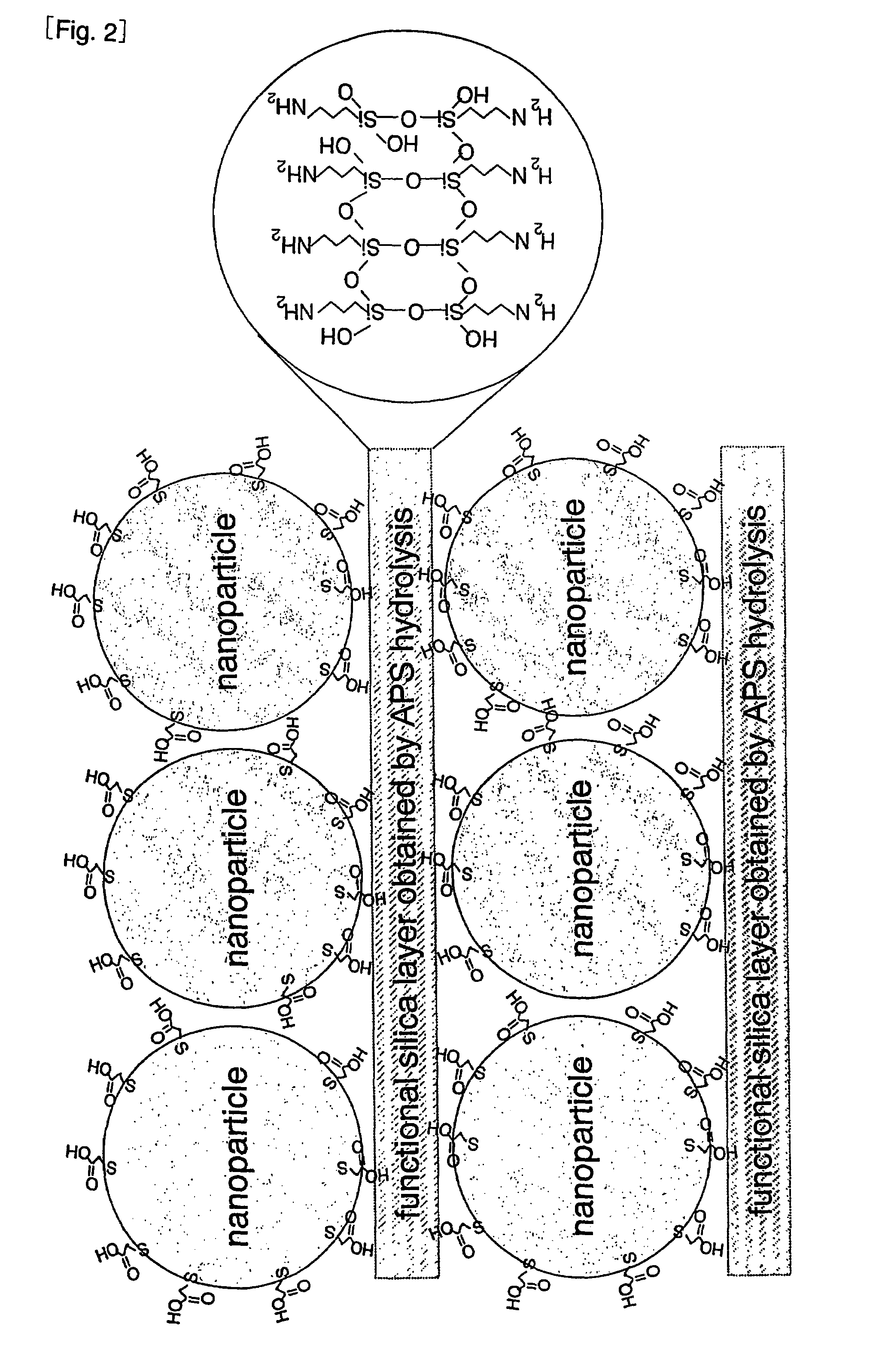
[0139]A glass thin film with a dispersion of cadmium telluride nanoparticles emitting red light was manufactured by the layer-by-layer method using aminopropyltrimethoxysilane (APS).

[0140]The cadmium telluride nanoparticles were manufactured in accordance with an existing method (Li, Murase, Chemistry Letters, volume 34, page 92, 2005). More specifically, cadmium perchlorate (hexahydrate, 1.095 g) was dissolved in 200 ml of water. To this, thioglycolic acid, (TGA) as a surfactant, was added in an amount of 1.5 times the mols of cadmium perchlorate. To the result, 1 N aqueous solution of sodium hydroxide was added to adjust the pH to 11.4. After degassing for 30 minutes, hydrogen telluride gas was introduced in an inert atmosphere while stirring vigorously. After stirring for 10 minutes, a condenser was attached for refluxing at about 100° C. Cadmium telluride particles grew by refluxing, and the wavelength of emitted light shifted from green to red.

[0141]First, refluxing was suffici...

example 2

[0150]The same procedure as in Example 1 was followed except that the slide glass was immersed in an aqueous solution of thioglycolic acid (TGA), i.e., “solution 2” for about 7 minutes, thereby manufacturing a thin-film fluorescent material with a dispersion of nanoparticles having a concentration of the nanoparticles in the thin film of 4×10⁻³ mol / l and having a fluorescence quantum yield of 25%.

[0151]Thus, it was found that a glass thin film whose concentration is 10−3 mol / l order and which has a fluorescence quantum yield exceeding 20% was obtained by the layer-by-layer method.

example 3

[0152]The same procedure as in Example 1 was followed except that the lamination cycle was repeated 40 times, thereby manufacturing a thin-film fluorescent material with a dispersion of nanoparticles having a concentration of the nanoparticles in the thin film of 9×10⁻³ mol / l and having a fluorescence quantum yield of 21%. In this case, it was confirmed that the film thickness of the fluorescent material was about 0.2 μm.


PUM

PropertyMeasurementUnit
diameteraaaaaaaaaa
fluorescence quantum yieldaaaaaaaaaa
thicknessaaaaaaaaaa

Abstract

The present invention provides a thin-film fluorescent material in which semiconductor nanoparticles in a stable condition maintain a high fluorescence quantum yield and can be held at a high concentration in a glass matrix. The present invention also provides optical devices using the thin-film fluorescent material, such as high-brightness displays and lighting systems. The present invention relates to a fluorescent material, in which semiconductor nanoparticles with a fluorescence quantum yield of 15% or more and a diameter of 2 to 5 nanometers are dispersed in a glass matrix at a concentration of 5×10⁻⁴ mol / l or more and a method for manufacturing the same.

Description

TECHNICAL FIELD[0001]The present invention relates to a fluorescent material with semiconductor nanoparticles dispersed therein, a method for manufacturing the same, and light-emitting devices (lighting systems, displays, etc.) using the fluorescent material.BACKGROUND OF THE INVENTION[0002]Nowadays, fluorescent materials are widely used as illumination or display materials, and support our daily lives. Among such fluorescent materials, inorganic matrices with coloring materials and / or transition element ions (transition-metal ions and / or rare earth ions) have been in use for a long time.[0003]In recent years, it has been discovered that semiconductor nanoparticles obtained by a thoroughly researched manufacturing method emit light efficiently. Among such semiconductor nanoparticles, II-VI group compounds, such as cadmium telluride, and the like, are typically mentioned, and have a diameter of approximately 2 to 5 nanometers. Because semiconductor nanoparticles have a short emission...

Claims


Application Information

Patent Timeline
Patent Type & Authority Patents(United States)
IPC IPC(8): B32B5/16
CPCC09K11/08Y10T428/25Y10S977/778Y10T428/256Y10T428/261
Inventor MURASE, NORIOYANG, PING
Owner NAT INST OF ADVANCED IND SCI & TECH
Why Eureka
Try Eureka