Electrical fuse having a cavity thereupon
a technology of electrical fuse and cavity, applied in the direction of transistors, semiconductor/solid-state device details, instruments, etc., can solve the problems of adverse effects on the performance of many semiconductor devices, and achieve the effects of less programming current, enhanced thermal isolation of electrical fuse, and superior thermal isolation
- Summary
- Abstract
- Description
- Claims
- Application Information
AI Technical Summary
Benefits of technology
Problems solved by technology
Method used
Image
Examples
first embodiment
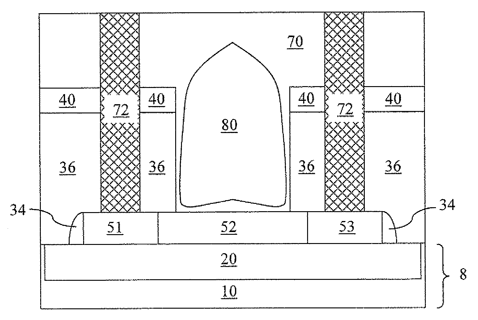
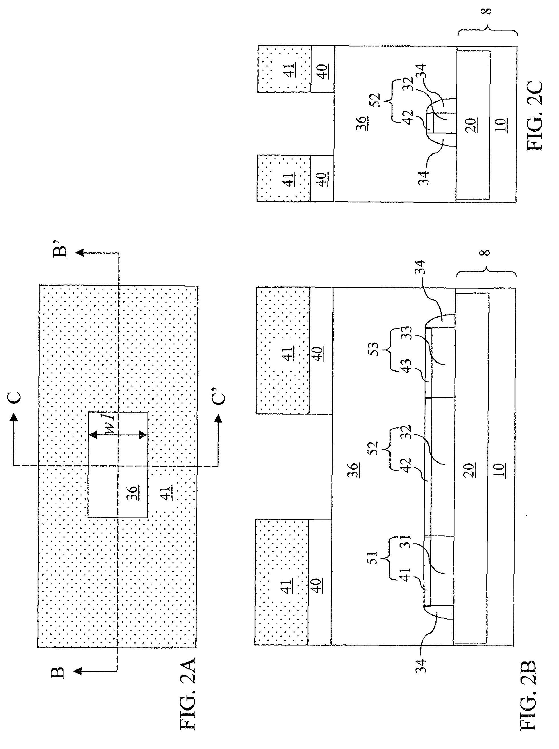
[0070]An optional dielectric cap layer 40 may be deposited on the first dielectric layer 40. The thickness of the optional dielectric cap layer 40 may be from about 5 nm to about 200 nm, and typically from about 20 nm to about 50 nm. The optional dielectric cap layer 40 may comprise a silicon oxide, a silicon nitride, or a stack thereof. In a variation of the first embodiment, the optional dielectric cap layer is omitted so that the photoresist 41 is applied directly on the first dielectric layer 36.
[0071]A photoresist 41 is applied on the optional dielectric cap layer 40 and lithographically patterned to expose a portion of the optional dielectric cap layer 40 over the fuselink 52. An opening having a lithographic dimension is patterned in the photoresist 41. The opening may be rectangular and may have a first lithographic width w1 in the direction perpendicular to the direction between the first electrode 51 and the second electrode 53. The first lithographic width w1 may be great...
second embodiment
[0086]A second exemplary structure according to the present invention is derived from the first exemplary structure shown in FIGS. 2A-2C by reducing the first lithographic width w1. Specifically, the opening formed in the photoresist 41 (See FIGS. 2A-2C) has a second lithographic width w2 in the direction perpendicular to the direction between the first electrode 51 and the second electrode 53. The second lithographic width w2 is a lithographic dimension, i.e., is equal to or greater than the lithographic minimum dimension. The second lithographic dimension w2 is less than the sum of the width of the fuselink 52 and twice the width of the dielectric spacer 34.
[0087]Referring to FIGS. 7A-7C, the optional dielectric cap layer 40 and the first dielectric layer 36 are etched to form an opening in the first dielectric layer 36 as in the first embodiment. A top surface of the fuselink 52 and a top surface of portions of the dielectric spacer 34 are exposed within the opening in the first ...
fourth embodiment
[0096]Referring to FIGS. 13 A-13C, a fifth exemplary semiconductor structure is formed by etching at least one additional volume of the first dielectric layer 36 connecting portion of the opening in the first dielectric layer 36 around the periphery of the electrical fuse (51, 52, 53) of the fourth exemplary structure in FIGS. 11A-11C. The cavity encircles a first portion of the first dielectric layer 36 located above the first electrode 51, a second portion of the first dielectric layer 36 located above the second electrode 52, and a third portion of the first dielectric layer 36 located above the fuselink 52. The opening in the first dielectric layer 36 comprises multiple trenches that are interconnected. The opening may have substantially the same width, which is the fourth lithographic dimension w4, or may have a local variation. The width of the opening, i.e., the lateral dimension between two opposing sidewalls of the first dielectric layer in the opening, is lithographic as i...
PUM
 Abstract
Description
Claims
Application Information


