Thermopile infrared sensor array

a technology of infrared sensor array and thermoplastic, which is applied in the field of thermoplastic infrared sensor array, can solve the problems of high manufacturing cost, significant increase of sensor cost, and shift of detection limit (thermal resolution) to higher temperatures

Active Publication Date: 2010-11-30
HEIMANN SENSOR GMBH
View PDF17 Cites 30 Cited by
  • Summary
  • Abstract
  • Description
  • Claims
  • Application Information

AI Technical Summary

Benefits of technology

[0030]A particularly good thermal resolution capacity is achieved by the invention and thermal influencing of the thermal biosensor elements by the power loss of the necessary electronic components, like preamplifiers, is minimized.
[0036]To avoid damage to the membrane by overpressure or underpressure in the recess after mounting of the chip on the support substrate, a thin ventilation slit can be provided through the separation walls and through the solid edge area at least for each row or column.
[0045]It is also advantageous if the cap has a surface that absorbs infrared radiation on the side facing the sensor elements.

Problems solved by technology

Since the sensor and preamplifier noise is influenced by the bandwidth of this preamplifier, fairly high noise is obtained, which shifts the detection limit (thermal resolution) to higher temperatures.
The sensor chips achieved with the presented wet etching technology are relatively large, which leads to high manufacturing costs.
Vacuum-tight housings, however, increase the sensor costs significantly and limit the applicability for cheap high-volume applications.
The monolithic 16×16 array chip presented by Schaufelbühl, A., Münch, U. with 7.4×12 mm is also fairly large and costly to produce.
If, however, individual preamplifiers are arranged outside of the sensor chip, the space requirements and manufacturing costs are further increased.
The size of the chip related to the process leads to relatively high manufacturing costs and again stands in the way of cost-effective mass applications.
However, the small element dimensions on the silicon surface necessarily require vacuum-tight packing of the sensor chip, which again stands in the way of cost-effective mass production.
However, the hybrid technology increases the costs in comparison with monolithic sensor arrangements in silicon technology.
In addition, pyroelectric sensors generally have the drawback that they only respond to varying objects.
Additional mechanically moved parts reduce the reliability and increase the mechanical size as well as the costs of an infrared sensor array.
In the prior art cited above thermal infrared sensor arrays are proposed, which have cost drawbacks for production of infrared sensor arrays in large numbers eitherbecause of a large-surface chip technology (A. D. Oliver, K. D. Wise, Schaufelbühl, A., Münch, U., Münch, U. et al. and Horiba product information)a costly vacuum housing technology (Kanno, T. et al., Masaki Hirota et al., B. E. Cole, C. J. Han and Oda, Naoki oran additional mechanical chopper assembly.

Method used


Image

  • Thermopile infrared sensor array
  • Thermopile infrared sensor array
  • Thermopile infrared sensor array

Examples


Embodiment Construction

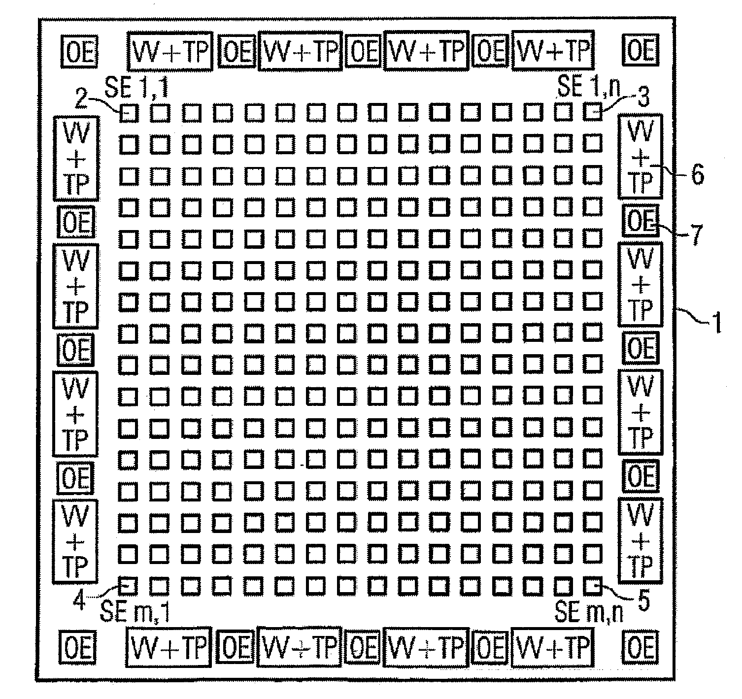
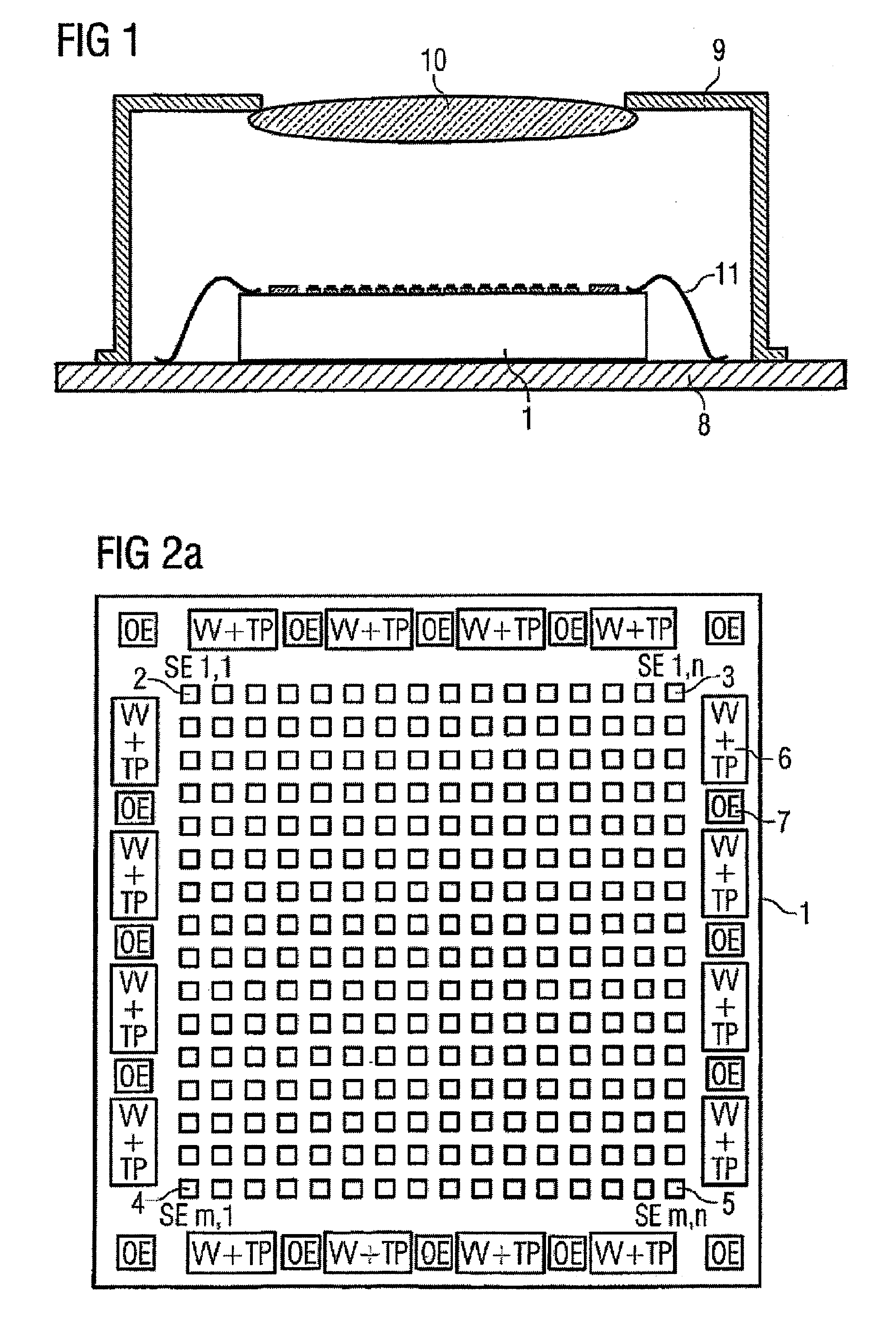
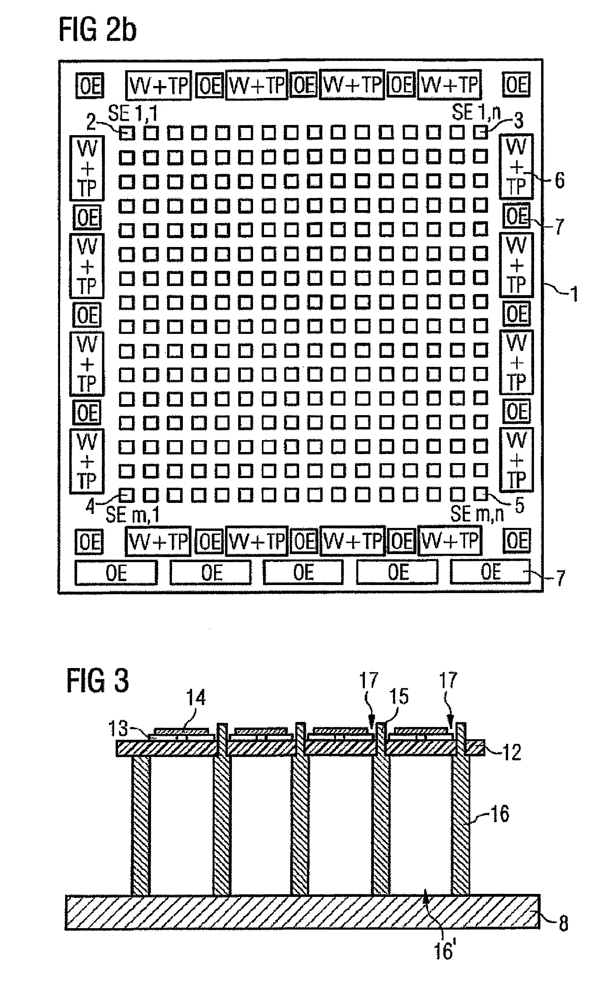
[0064]The thermopile sensor array chip (referred to subsequently as sensor chip 1) is applied centrally according to FIG. 1 on a support substrate 8, for example a bottom plate, and covered with a cap 9. The cap 9 contains an opening for the inlet optics 10, which is arranged precisely above the center of the sensor elements of sensor chip 1. The inlet optics 10 can be a plane-parallel filter or a lens optics on one side. The connection between the sensor chip 1 and the support substrate 8 can be produced by joining by gluing, soldering, glazing or also by welding. The joining method should have very high heat conductivity. An adhesive filled with metal or ceramic, a metal-filled glazing or solder is suitable as joining method.

[0065]The variant with filter is not shown in FIG. 1 and in this case a lens must be additionally mounted outside of the housing.

[0066]In the variant depicted in FIG. 1 an imaging lens is provided as inlet optics 10. The dimensions of cap 9, sensor chip 1 and ...


PUM


Abstract

A thermopile infrared sensor array, comprises a sensor chip with a number of thermopile sensor elements, made from a semiconductor substrate and corresponding electronic components. The sensor chip is mounted on a support circuit board and enclosed by a cap in which a lens is arranged. The aim is the production of a monolithic infrared sensor array with a high thermal resolution capacity with a small chip size and which may be economically produced. The aim is achieved by arranging a thin membrane made from non-conducting material on the semiconductor substrate of the sensor chip on which the thermopile sensor elements are located in an array. Under each thermopile sensor element, the back side of the membrane is uncovered in a honeycomb pattern by etching and the electronic components are arranged in the boundary region of the sensor chip. An individual pre-amplifier with a subsequent low-pass filter may be provided for each column and each row of sensor elements.

Description

CROSS REFERENCE TO RELATED APPLICATIONS[0001]This application is a national stage filing under section 371 of PCT International Application No. PCT / DE2006 / 000841, filed on May 16, 2006, and published in German on Nov. 23, 2006 as WO2006 / 122529 A2, and claims priority from German patent application No. 10 2005 023 333.3, filed on May 17, 2005, the entire disclosure of these applications being hereby incorporated herein by reference.BACKGROUND ART[0002]The invention concerns a thermopile infrared sensor array consisting of a sensor chip with a number of thermopile sensor elements constructed on a semiconductor substrate of a sensor chip and corresponding electronic components, like preamplifiers, addressing devices, in which the sensor chip is mounted on a support substrate and closed with a cap in which inlet optics is situated in the center above the sensor chip.[0003]Infrared sensors that can be produced in Si micromachining are known in various types.[0004]For example, a monolithi...

Claims


Application Information

Patent Timeline
Patent Type & Authority Patents(United States)
IPC IPC(8): G01J5/16G01J5/04G01J5/12
CPCG01J5/06G01J5/12H04N5/2253H04N5/33H01L2924/3025H01L2224/48472H01L2224/48091H01L2924/1461H01L2924/00014H01L2924/00H04N23/54
Inventor LENEKE, WILHELMSIMON, MARIONSCHULZE, MISCHASTORCK, KARLHEINZSCHIEFERDECKER, JOERG
Owner HEIMANN SENSOR GMBH
Why Eureka
Try Eureka