Organic thin film transistor, method of manufacturing the same, and biosensor using the transistor

a technology of organic semiconductors and biosensors, which is applied in the direction of thermoelectric device junction materials, electrical apparatus, and semiconductor can solve the problem that the electronic and optical devices using organic semiconductors cannot completely replace conventional silicon-, and achieve the effect of high reliability and stability

Inactive Publication Date: 2011-01-04
ELECTRONICS & TELECOMM RES INST
View PDF9 Cites 2 Cited by
  • Summary
  • Abstract
  • Description
  • Claims
  • Application Information

AI Technical Summary

Benefits of technology

[0009]The present invention is directed to an organic thin film transistor (OTFT) having high reliability and stability.
[0010]Also, the present invention is directed to a method of manufacturing an OTFT having high reliability and stability.
[0011]Furthermore, the present invention is directed to a biosensor using an OTFT having high reliability and stability.

Problems solved by technology

Although electronic and optical devices using organic semiconductors cannot completely replace conventional silicon-based inorganic devices, they are expected to overcome certain weaknesses of inorganic devices and create new fields of application.

Method used


Image

  • Organic thin film transistor, method of manufacturing the same, and biosensor using the transistor
  • Organic thin film transistor, method of manufacturing the same, and biosensor using the transistor
  • Organic thin film transistor, method of manufacturing the same, and biosensor using the transistor

Examples


embodiment 1

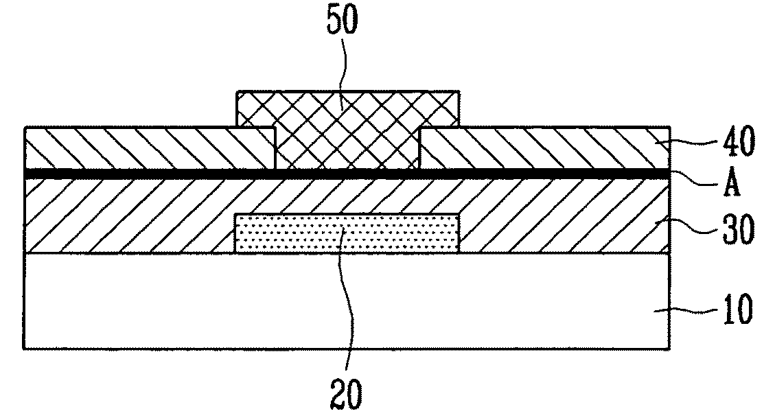
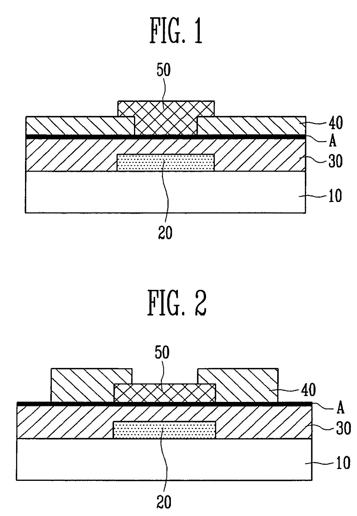
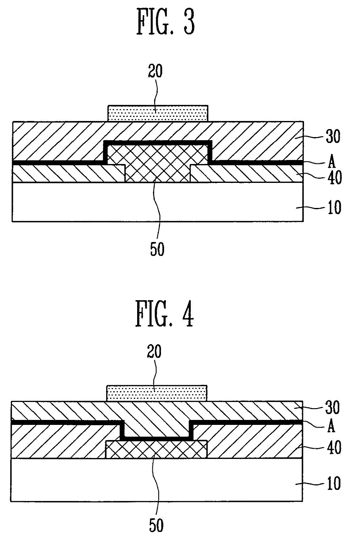
[0049]A gate electrode was formed by depositing a Au layer to a thickness of about 100 nm on a PES substrate processed with O2-plasma by a lithography process using an electronic beam (e-beam) apparatus and patterning the deposited Au layer. 1 g of PVP was sufficiently dissolved in 10 ml of DMF by stirring, 0.03 g of ammonium dichromate was added to a PVP solution, and the PVP solution containing ammonium dichromate was sufficiently mixed for 2 hours by stirring. Thereafter, the PVP solution was filtered using a 0.2-mm filter to minimize fine particles, and then spin-coated on the gate electrode for 180 seconds at a rate of 2500 rpm. The coated PVP solution was sufficiently maintained at room temperature in a vacuum state of about 10−1 Torr for 16 hours to evaporate an organic solvent, thereby forming a gate insulating layer to a thickness of about 80 nm. After that, the PES substrate was exposed to a dose of about 240 mJ / cm2 of ultraviolet (UV) radiation for 8 minutes using a photo...


PUM


Abstract

An organic thin film transistor (OTFT), a method of manufacturing the same, and a biosensor using the OTFT are provided. The OTFT includes a gate electrode, a gate insulating layer, source and drain electrodes, and an organic semiconductor layer disposed on a substrate and further includes an interface layer formed between the gate insulating layer and the organic semiconductor layer by a sol-gel process. The gate insulating layer is formed of an organic polymer, and the interface layer is formed of an inorganic material. The OTFT employs the interface layer interposed between the gate insulating layer and the organic semiconductor layer so that the gate insulating layer can be protected from the exterior and adhesion of the gate insulating layer with the organic semiconductor layer can be improved, thereby increasing driving stability. Also, since the OTFT can use a plastic substrate, the manufacture of the OTFT is inexpensive so that the OTFT can be used as a disposable biosensor.

Description

CROSS-REFERENCE TO RELATED APPLICATION[0001]This application claims priority to and the benefit of Korean Patent Application No. 2008-42244, filed May 7, 2008, and Korean Patent Application No. 2008-71203, filed Jul. 22, 2008, the disclosure of which is incorporated herein by reference in its entirety.BACKGROUND[0002]1. Field of the Invention[0003]The present invention relates to an organic thin film transistor (OTFT), a method of manufacturing the same, and a biosensor using the OTFT, and more specifically, to an OTFT in which an interface layer is interposed between an organic gate insulating layer and an organic semiconductor layer to protect the organic gate insulating layer from the exterior and improve adhesion of the organic gate insulating layer with the organic semiconductor layer to thereby increase driving stability, a method of manufacturing the OTFT, and a biosensor using the OTFT.[0004]2. Discussion of Related Art[0005]In recent years, a vast amount of research has bee...

Claims


Application Information

Patent Timeline
Patent Type & Authority Patents(United States)
IPC IPC(8): H01L51/40
CPCH01L51/0533H01L51/0562H01L51/0097H01L51/0541H01L51/0545H10K77/111H10K10/476H10K10/486H10K10/466H10K10/464
Inventor LIM, SANG CHULKIM, SEONG HYUNYANG, YONG SUKYOUN, DOO HYEBKIM, ZIN SIG
Owner ELECTRONICS & TELECOMM RES INST
Why Eureka
Try Eureka