Single photon source

a single photon source and photon source technology, applied in the field of optical communication devices, can solve the problems of poor collection efficiency, low repetition rate, and difficulty in fabricating arrays of multiple quantum dots precisely, and achieve the effect of improving the accuracy of the array

Inactive Publication Date: 2011-02-15
ECOLE POLYTECHNIQUE FEDERALE DE LAUSANNE (EPFL)
View PDF6 Cites 1 Cited by
  • Summary
  • Abstract
  • Description
  • Claims
  • Application Information

AI Technical Summary

Benefits of technology

[0004]According to the present invention a microcavity is provided which comprises two reflectors, at least one semiconductor layer separating said reflectors and at least one semiconductor quantum well wherein at least one of said reflectors and of said semiconductor layer comprises a structure which is adjusted to spatially localize, i.e. to produce a preferably three dimensional quantum confinement of a polariton or an optical polariton excitation, respectively, in said microcavity. The inventive microcavity allows the formation of quasi-particles called cavity polaritons, consisting of the quantum superposition of an exciton, i.e. a two-particle state of a correlated electron-hole pair in a quantum well and a photon. In order to permit the generation of polaritons the length of the cavity formed between the reflectors is such that a microcavity photonic mode with a frequency close to the emission frequency of an exciton in the quantum well is formed. Preferably the cavity length or thickness corresponds to an integer multiple of the wave length of radiation emitted by an exciton formed in the quantum well. Due to the structure of the inventive microcavity which is adjusted to localize or locally confine a polariton in at least one region thereof, the fundamental polariton energy state (the polariton state with the lowest possible energy) of the localized polariton(s) becomes blocked for the absorption of a photon with a wavelength which is resonant to the fundamental polariton energy state when the fundamental energy state is occupied preferably with a single polariton only. After the emission of a single photon within the radiative lifetime of the polariton the fundamental polariton state is free and a photon can be absorbed to newly generate a polariton.
[0009]According to a further embodiment a local change of the length of the cavity can be achieved by providing at least one reflector and / or semiconductor layer in said cavity which comprises a raised or recessed region in one of the surfaces and preferably in one of the surfaces which are oriented perpendicular to the longitudinal dimension of the microcavity_to locally change and preferably increase the length of the cavity in that region. Such a structure can be fabricated by lithographic and etching techniques commonly used in semiconductor technology. It is preferred to obtain a cavity with a locally modified length by preparing a spacer layer of the microcavity with a raised region on top of which further semiconductor layers e.g. of a Bragg mirror are grown. According to a preferred embodiment at least one of said reflectors is a Bragg reflector including a sequence of alternating semiconductor layers having different band gaps. Bragg reflectors can conveniently be produced using well known semiconductor fabrication technologies. The raised region in the spacer layer is preferably transferred to the semiconductor layers of the Bragg reflector subsequently grown on top of it. Alternatively a raised or recessed region could be formed in one of the layers of the Bragg reflector. In addition, it can also be taken into account to provide a layer including a raised or projecting region on both sides of the microcavity with the raised structures oppositely oriented towards the respective end of the microcavity.
[0015]Due to the localization of a polaritons in the microcavity according to the inventive method an energy shift of the renormalized fundamental polariton-energies towards higher energies in the case of more than one polariton occupying the localizing structure of the microcavity is obtained. Thus a quantum blocking effect which prevents a absorption of photons with a wavelength which is resonant with the fundamental energy state of a single localized polariton in the microcavity is achieved. By irradiating the microcavity with a wavelength which is resonant with the fundamental single-polariton energy state, a single photon absorption process is produced. Thereupon, within the lifetime of the polariton, a single photon emission process with a repetition rate corresponding to the lifetime of the localized polariton follows. It becomes possible to obtain a beam of single photons with a high repetition rate of preferably up to 10 GHz and a collection efficiency close to 100%.

Problems solved by technology

However, such a source suffers from random fluctuations in the photon emission rate which means major drawbacks for a use as an optical telecommunication device.
An example of an optically driven quantum dot photon source is given in GB 2377551 A. Although single quantum dot sources are advantageous in respect of their compactness they include the drawback of a poor collection efficiency and a low repetition rate.
Moreover, it is difficult to fabricate arrays of multiple quantum dots with precisely predetermined positions of the dots with present manufacturing methods such as self-assembling techniques.

Method used


Image

  • Single photon source
  • Single photon source
  • Single photon source

Examples


Embodiment Construction

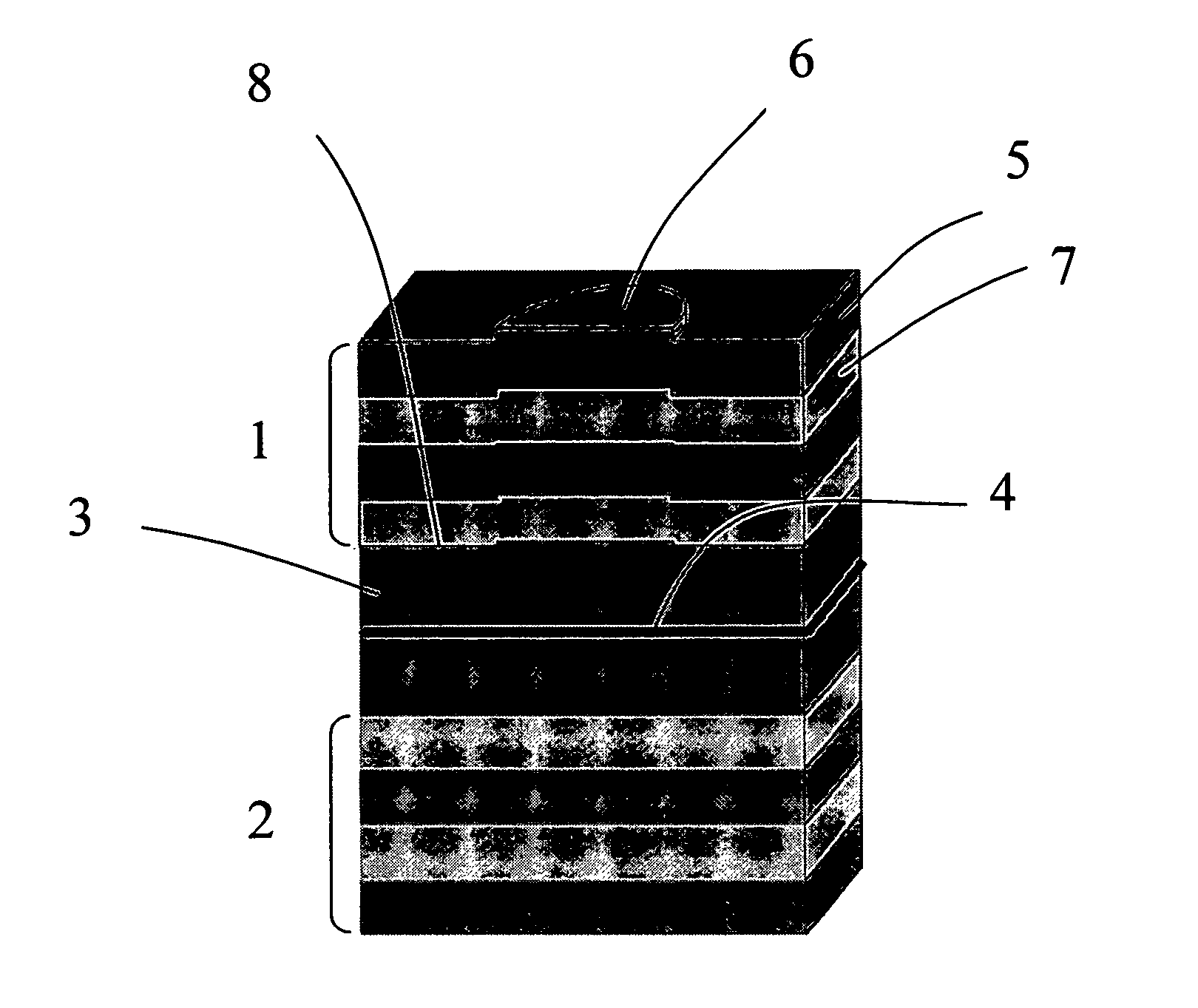
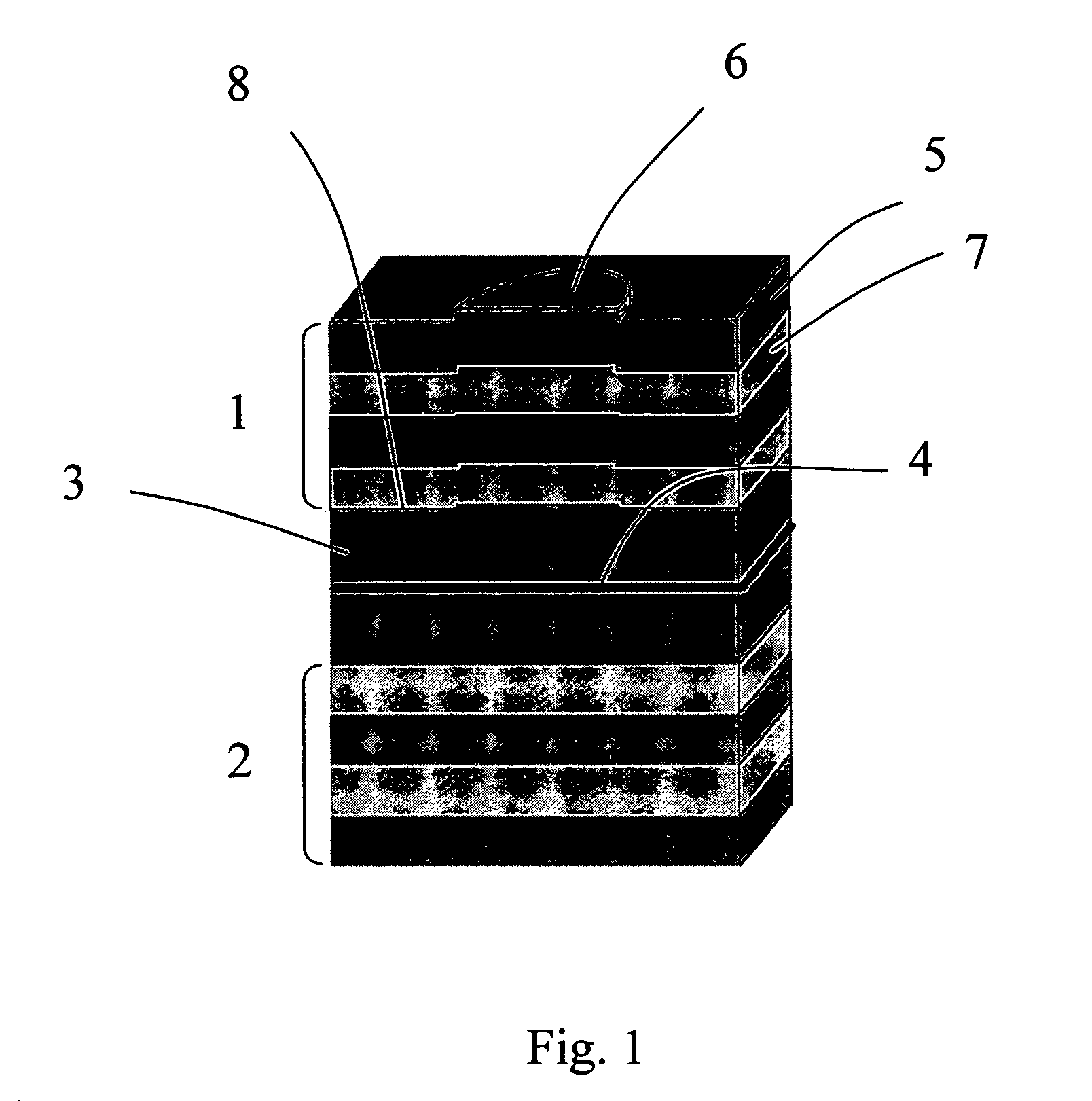
[0025]FIG. 1 shows an example of a microcavity comprising two Bragg reflectors 1, 2 formed of alternating layers 5, 7 of GaAs and AlAs. The Bragg reflectors 1, 2 are separated by two semiconductor layers 3 of GaAs that surround a single quantum well of In0.04Ga0.96As. Its fundamental energy level corresponds to a wavelength of 835 nm. The distance between the Bragg reflectors corresponds to this wavelength. Therefore, the formation of a polariton, i.e. the superposition of a photon and an exciton in the microcavity is granted. The semiconductor layers are sequentially grown on a substrate (not shown) using molecular beam epitaxy (MBE). For the purpose of illustration only a reduced number of the semiconductor layers of the actually grown microcavity and of the semiconductor layers forming the Bragg reflectors 1, 2 are shown. The Bragg reflectors each comprise a reflectivity of more than 99.5%. The microcavity can also include more than one quantum well, wherein the number of quantum...


PUM


Abstract

Microcavity comprising two reflectors, at least one semiconductor layer separating said reflectors and a semiconductor quantum well wherein at least one of said reflectors and of said at least one semiconductor layer comprises a structure which is adjusted to localize a polariton in said microcavity.

Description

FIELD OF INVENTION[0001]This invention generally relates to optical communication devices and in particular to a single photon source and a corresponding method.BACKGROUND OF INVENTION[0002]A single photon source is a light source which is adjusted to repetitively emit single photons at a specific repetition rate. It can be used e.g. in optical quantum cryptography. One way of realizing a single photon source is to attenuate a laser beam down to a level where emitted photons are statistically separated with a sufficient probability. However, such a source suffers from random fluctuations in the photon emission rate which means major drawbacks for a use as an optical telecommunication device. According to another type of single photon source an optically or electrically driven emission from a single quantum dot is used. An example of an optically driven quantum dot photon source is given in GB 2377551 A. Although single quantum dot sources are advantageous in respect of their compact...

Claims


Application Information

Patent Timeline
Patent Type & Authority Patents(United States)
IPC IPC(8): H01L33/00
CPCH01S5/18327H01S5/041H01S5/423
Inventor DEVEAUD-PLEDRAN, BENO TCIUTI, CRISTIANOMORIER-GENOUD, FRANCOIS
Owner ECOLE POLYTECHNIQUE FEDERALE DE LAUSANNE (EPFL)
Why Eureka
Try Eureka