Optical delay line interferometer

a technology of optical delay line and interferometer, which is applied in the direction of optical elements, optical waveguide light guides, instruments, etc., can solve the problems of significant degradation of the s/n ratio of demodulated signals, achieve the reduction of polarization dependence and temperature eliminate the polarization dependence of optical delay line interferometer, resulting from birefringence and polarization coupling.

Active Publication Date: 2011-03-01
NIPPON TELEGRAPH & TELEPHONE CORP
View PDF14 Cites 22 Cited by
  • Summary
  • Abstract
  • Description
  • Claims
  • Application Information

AI Technical Summary

Benefits of technology

[0032]Generally, the elimination of the polarization dependence in the optical delay line interferometer with a simple configuration such as is shown in FIG. 1 can be accomplished by the placement of a polarization converter in the optical delay line interferometer (See Patent Document 3). The polarization converters include, for example, a half-wave plate whose optic axis is inclined by 45° relative to an optic axis of the waveguide. The half-wave plate whose optic axis is inclined by 45° relative to the optic axis of the waveguide will be hereinafter called merely a “half-wave plate.” By the utilization of the half-wave plate for conversion from one to another of TE and TM polarizations, the effective refractive index sensed by the propagating light can be regarded as an average value of the effective refractive indices for the TE polarization and the TM polarization, respectively. Thus, the placement of the polarization converter in the optical delay line interferometer enables the elimination of the polarization dependence of the optical delay line interferometer.
[0042]FIG. 6C shows transmission spectrum in a case where the temperature undergoes the ΔT change when the grooves 14 in the two Mach-Zehnder interferometers have fabrication error but has the same fabrication error. Although the temperature dependence of each Mach-Zehnder interferometer is not completely eliminated, the temperature dependence is reduced by the same amount. Thus, each transmission spectrum shifts along the wavelength axis, but the phase difference between the transmission spectrums is held at π / 2. Therefore, in this instance, the cause of the deterioration in the reception characteristics of the demodulator is only an offset between wavelengths λs and λc of the optical signal. The variable phase adjuster, added to the long arm waveguides 4a and 4b or the short arm waveguides 5a and 5b, enables easily the wavelengths λs and λc to coincidence with each other.
[0046]On the other hand, the DQPSK demodulator shown in the conventional art 3 uses one Mach-Zehnder interferometer alone, and thus, the groove 14 may be formed in one location. The uniformity in the fabrication error of the groove width w presents no problem, as distinct from the configuration of the conventional art 2 in which the grooves 14 are formed in two locations. However, as mentioned above, the configuration of conventional art 3 has difficulty in eliminating the polarization dependence of the optical delay line interferometer.
[0050]The present invention has been made in view of the foregoing problems, and an object of the present invention is to eliminate the polarization dependence of the optical delay line interferometer, resulting from the birefringence and the polarization coupling. The present invention proposes a circuit configuration suitable for making polarization-independent the optical delay line interferometer in which the polarization converter is disposed. Another object of the present invention is to provide an optical delay line interferometer in which the polarization dependence of optical characteristics is small and further, the temperature dependence of the optical characteristics is small. The present invention proposes a circuit configuration suitable for eliminating both the polarization dependence and the temperature dependence of the optical delay line interferometer. Further proposed is the configuration of the demodulator formed by the optical delay line interferometer, in which the S / N ratio of the demodulated signal is improved.
[0053]Further, the optical delay line interferometer may further includes grooves each formed in line by removing a portion of a cladding and a portion of a core that form each of at least either the N long arm waveguides or the N short arm waveguides, while extending across the at least either the N long arm waveguides or the N short arm waveguides, the grooves being filled with a material having a different coefficient of refractive index dependence on temperature from a coefficient of effective refractive index dependence on temperature of the waveguides, thereby to compensate for a variation in loss spectrum in a wavelength axis due to a change in temperature of the N interferometers.
[0063]According to the present invention, the polarization dependence of the optical delay line interferometer, resulting from the birefringence and the polarization coupling, can be eliminated. Provided is the circuit configuration suitable for making polarization-independent the optical delay line interferometer in which the polarization converter is disposed. Provided is the demodulator formed by the optical delay line interferometer, in which the S / N ratio of the demodulated signal is improved. Further, according to the present invention, both the polarization dependence and the temperature dependence of the optical delay line interferometer can be reduced. The disposition of the polarization converter and the grove filled with the temperature compensation material makes it possible to provide the circuit configuration suitable for eliminating the polarization dependence and the temperature dependence of the optical delay line interferometer. Further, a circuit arrangement with high symmetry can be achieved, and the PDf resulting from the polarization coupling-induced light can be effectively eliminated.

Problems solved by technology

However, a waveguide-type optical circuit generally has birefringence, and thus, the interference and other characteristics of the optical delay line interferometer vary depending on the state of polarization of an input optical signal.
A variation in the interference characteristics, depending on the state of polarization of the input optical signal, leads to the problem of causing significant degradation of the S / N ratio of a demodulated signal at the time of demodulation of a DPSK optical signal.
A second cause is that the birefringence results from operation of the variable phase adjuster for fine adjustment of the delay time or the like in the optical delay line interferometer.

Method used


Image

  • Optical delay line interferometer
  • Optical delay line interferometer
  • Optical delay line interferometer

Examples


first embodiment

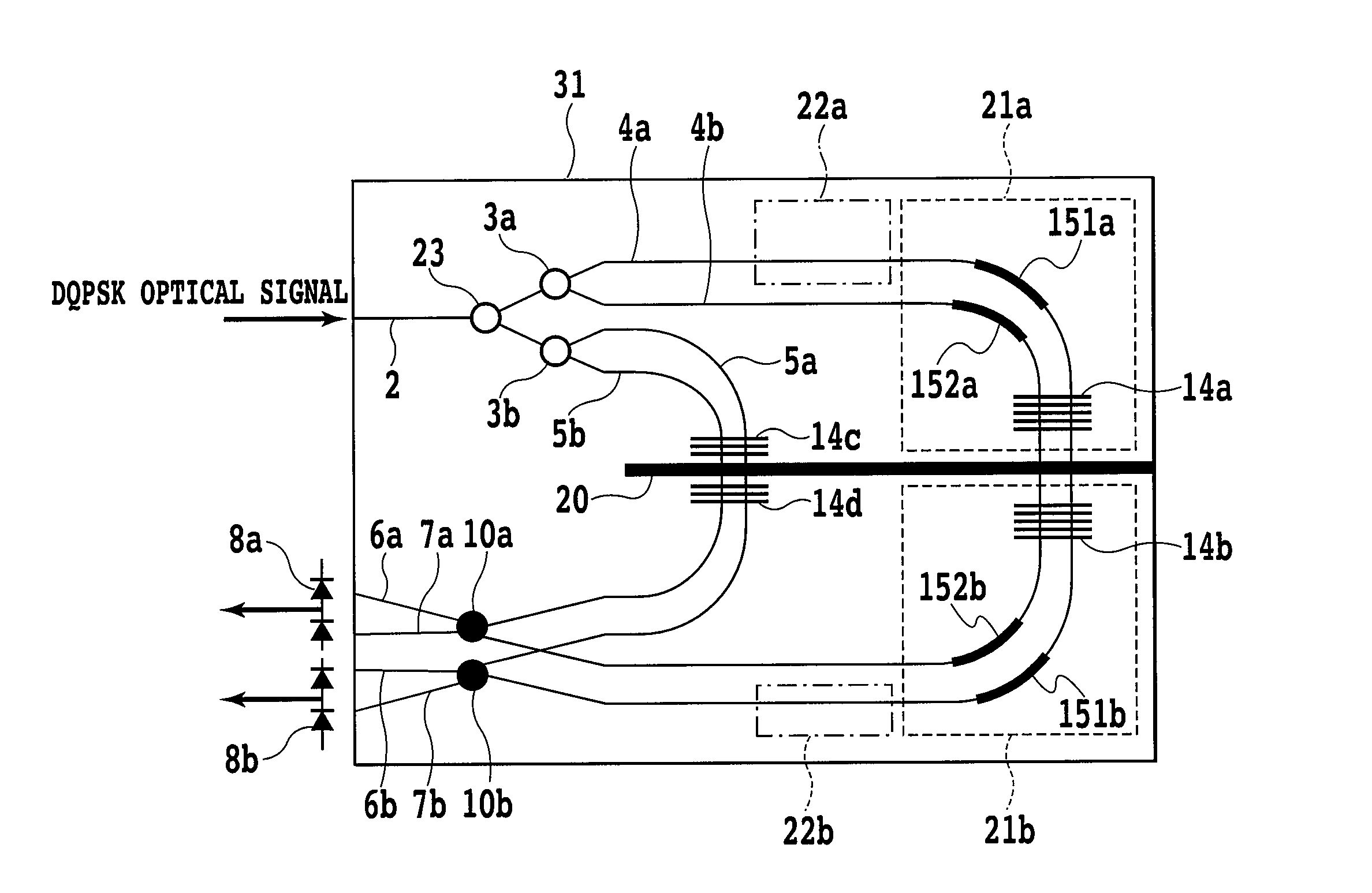
[0129]FIG. 14 shows a schematic diagram of an optical delay line interferometer according to the first embodiment, fabricated actually. The PLC technology is used for fabrication of the optical delay line interferometer. Specifically, flame hydrolysis deposition and reactive ion etching are used to fabricate a silica glass waveguide on a silicon substrate. A core is 4.5 μm square in cross section, and a relative refractive-index difference is 1.5%. Overcladding glass of 30 μm thick is deposited to bury the core.

[0130]After deposition of the overcladding glass, a groove is formed by removing the cladding and the core in a portion of the long arm waveguide, using the reactive ion etching, and the formed groove is filled with the temperature compensation material. In the first embodiment, a silicone resin is used as the temperature compensation material; however, the present invention is not so limited, and, of course, a polymer material or the like may be used. The grooves 14a and 14b...

second embodiment

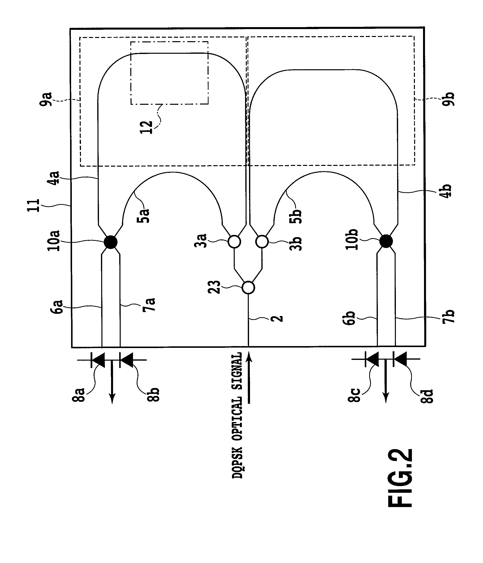
[0146]Two pairs of optical signals outputted from the optical delay line interferometer in the modulator for an optical multilevel differential phase shift keyed signal are demodulated by photoelectric converters (or the pair of balanced PDs). On this occasion, if there is an arrival time difference (or a skew) between the optical signals reaching the photoelectric converters, the optical signals are converted into electric signals at different times, and thus, demodulation distortion occurs at the time of phase demodulation. This has a great influence particularly on multileveled modulation with constellation points in close proximity to each other, which is not desirable for the demodulator. In order to compensate for the arrival time of the optical signals, a skew adjuster that adjusts the output timing of the optical signals may be placed at the output end of the optical delay line interferometer.

[0147]FIG. 22 is a block diagram of the optical delay line interferometer for DQPSK...

third embodiment

[0151]The embodiments described above are designed focusing on the elimination of the PDf caused by the birefringence and the elimination of the temperature dependence. Description will be given of an embodiment of the circuit configuration further capable of suppressing PDf deterioration caused by the polarization coupling, according to another aspect of the optical delay line interferometer of the present invention. Referring to this embodiment, description will be given of the circuit configuration designed to suppress the PDf by removing produced polarization coupling-induced light, not by suppressing the production in itself of polarization coupling-induced light.

[0152]In order to suppress the PDf caused by the polarization coupling, the simplest measurement is to suppress the production in itself of the polarization coupling-induced light that is the cause of the PDf deterioration. However, the suppression of the polarization coupling is very difficult. The polarization coupli...


PUM

PropertyMeasurementUnit
delay timeaaaaaaaaaa
refractive indexaaaaaaaaaa

Abstract

A demodulator is provided for a multilevel differential phase shift keyed signal, capable of eliminating polarization dependence due to birefringence and polarization coupling-induced light resulting from a waveguide structure, and also, polarization dependence due to dynamic birefringence produced at the time of driving a variable phase adjuster. The demodulator is configured of an optical delay line interferometer of a waveguide interference type. The S / N ratio of a demodulated signal in the demodulator formed by the optical delay line interferometer can be also improved. Further, both the polarization dependence and the temperature dependence of the optical delay line interferometer can be reduced. The disposition of a polarization converter and groves filled with a temperature compensation material makes it possible to provide a circuit configuration suitable for eliminating the polarization dependence and the temperature dependence of the optical delay line interferometer.

Description

TECHNICAL FIELD[0001]The present invention relates to an optical delay line interferometer that demodulates a phase-modulated optical signal and more particularly to an optical delay line interferometer having a low degree of polarization dependence.BACKGROUND ART[0002]As the optical communication technology moves forward, development of optical components configured to subject an optical signal directly to signal processing becomes increasingly important. Above all, a waveguide-type optical interferometer utilizing interference of light and using a planar lightwave circuit (PLC) integrated on a planar substrate, has advantageous features including mass production, low cost and high reliability, and many pieces of research and development thereof have been carried out. The waveguide-type optical interferometers include an arrayed waveguide diffraction grating, a Mach-Zehnder interferometer, and a lattice circuit, for example.[0003]Such waveguide-type optical interferometers are fabr...

Claims


Application Information

Patent Timeline
Patent Type & Authority Patents(United States)
IPC IPC(8): G02B6/12H04B10/00H04B10/516G02F2/00H04B10/61
CPCG02B6/12007G02B6/126H04B10/676G02B6/12011G02B6/12028G02B6/29355G02B6/29397G02B2006/12116G02B2006/12147G02B2006/1215
Inventor NASU, YUSUKEHATTORI, KUNINORIHASHIMOTO, TOSHIKAZUSAKAMAKI, YOHEITAKAHASHI, HIROSHIINOUE, YASUYUKI
Owner NIPPON TELEGRAPH & TELEPHONE CORP
Why Eureka
Try Eureka