Laminate device and module comprising same

a laminated inductors and magnetic circuit technology, applied in the direction of inductances, inductances with magnetic cores, cores/yokes, etc., can solve the problems of poor dc-superimposed characteristics of laminated inductors, drastic decreases in inductance, and limited miniaturization of laminated inductors, etc., to achieve stable inductance, excellent dc-superimposed characteristics, and easy production

Active Publication Date: 2011-03-15
HITACHI METALS LTD
View PDF28 Cites 27 Cited by
  • Summary
  • Abstract
  • Description
  • Claims
  • Application Information

AI Technical Summary

Benefits of technology

[0009]Accordingly, an object of the present invention is to provide an easily producible laminate device giving stable inductance in a range from small magnetization current to large magnetization current, with excellent DC-superimposed characteristics, and a module comprising such laminate device.DISCLOSURE OF THE INVENTION
[0010]As a result of intense research in view of the above object, the inventors have found that in a laminate device containing coil patterns, the formation of pluralities of magnetic gap layers in regions each in contact with the coil pattern makes magnetic saturation less likely in a magnetic material portion even with large magnetization current, resulting in decrease in eddy current loss. The present invention has been completed based on such finding.
[0014]With at least some of the coil patterns having more than one turn, the number of coil-pattern-carrying layers can be reduced. A coil pattern having more than one turn inevitably increases an area in which the coil pattern is formed, with a reduced cross section area of a magnetic path. However, the formation of a magnetic gap layer between adjacent coil patterns on a magnetic substrate layer provides inductance not smaller than that obtained when coil patterns having one turn or less are used. Such structure, however, makes magnetic saturation likely because of the reduction of a cross section area of a magnetic path, and increases floating capacitance between coil patterns opposing on the same magnetic substrate layer, thereby reducing a resonance frequency and lowering the quality coefficient Q of the coil. Accordingly, in the case of a 3216-size laminate device, for instance, a coil pattern on each layer preferably has 3 turns or less.
[0016]With at least some of the coil patterns having such structure, the laminate device has improved DC-superimposed characteristics. Magnetic gap layers in contact with all coil patterns provide stable inductance in a range from small magnetization current to large magnetization current, and excellent DC-superimposed characteristics, which keeps the inductance from lowering.
[0018]The magnetic gap layer preferably has at least one magnetic region. The magnetic region in the magnetic gap layer has such area and magnetic properties that it is more subjected to magnetic saturation with small magnetization current than in the magnetic layer between coil patterns adjacent in a lamination direction. With such structure, the inductance is high at small magnetization current, and lowers as the magnetization current becomes larger, but the magnetic region and the magnetic gap layer function as an integral magnetic gap, providing stable inductance.

Problems solved by technology

The inductor, one of passive parts, has conventionally been composed of a wire wound around a magnetic core, and its miniaturization is limited.
However, because it has an integral structure, magnetic saturation partially occurs in a magnetic material in the laminated inductor by a DC magnetic field generated when a magnetization current is applied to the coil pattern, resulting in drastic decrease in inductance.
Such laminated inductors have poor DC-superimposed characteristics.
Because most magnetic fluxes pass through the magnetic gap layer 44, this laminated inductor 50 has stable inductance in a range from small magnetization current to large magnetization current, but exhibits insufficient performance at large magnetization current.
In addition, it is difficult to produce because of a complicated structure.

Method used


Image

  • Laminate device and module comprising same
  • Laminate device and module comprising same
  • Laminate device and module comprising same

Examples


example 1

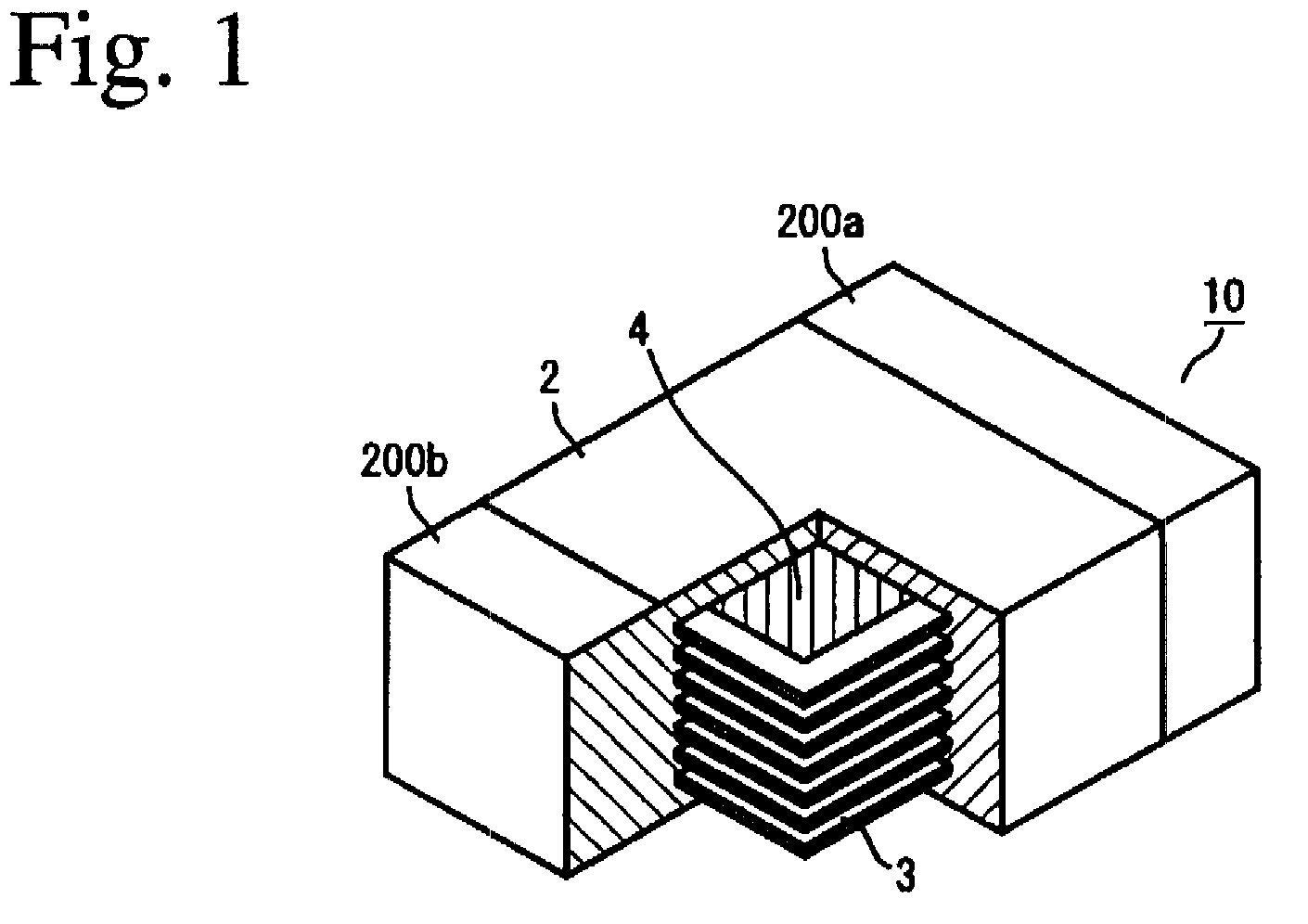
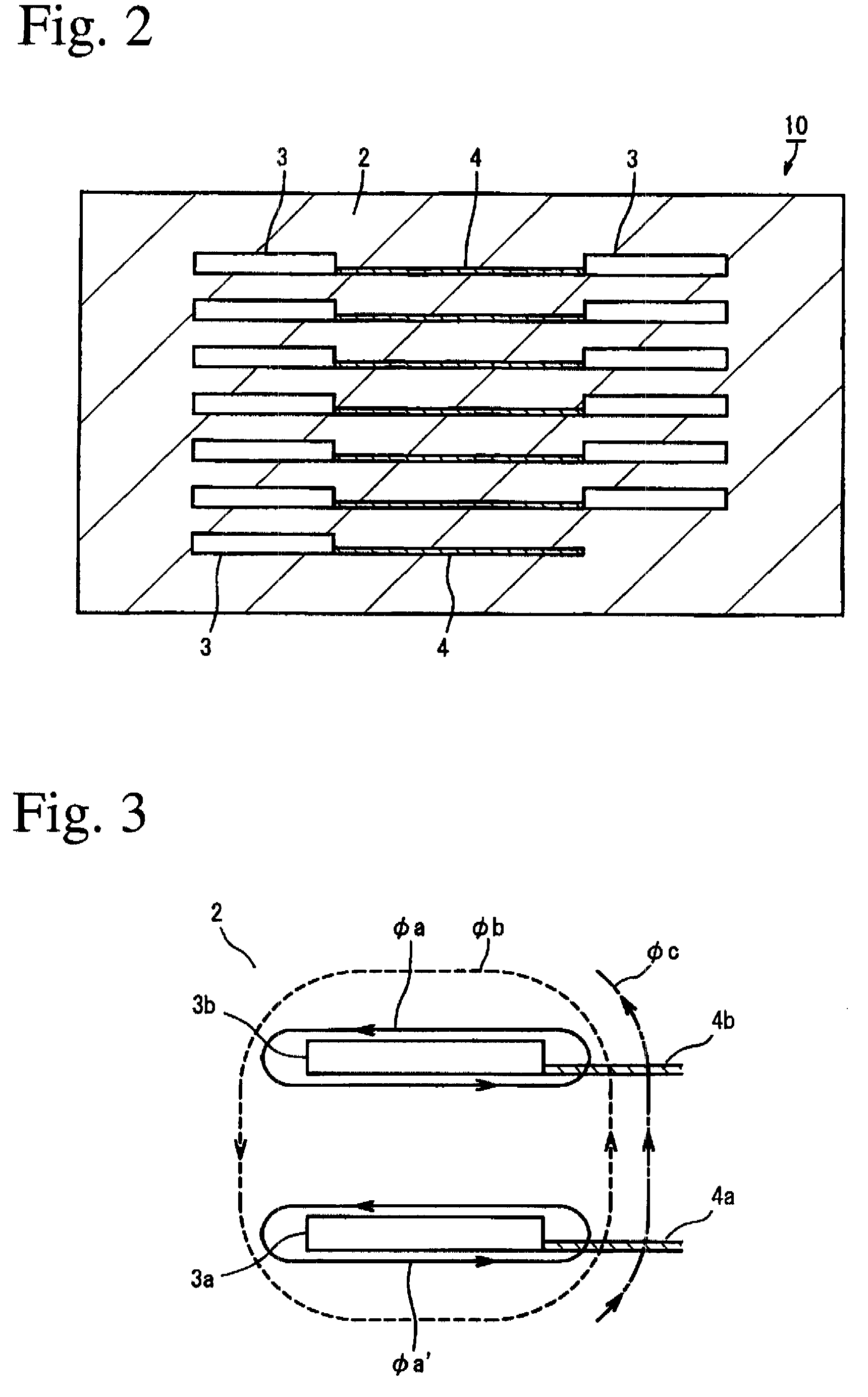
(1) Production of First Laminate Device Shown in FIGS. 1 to 6 (Sample A of Example)

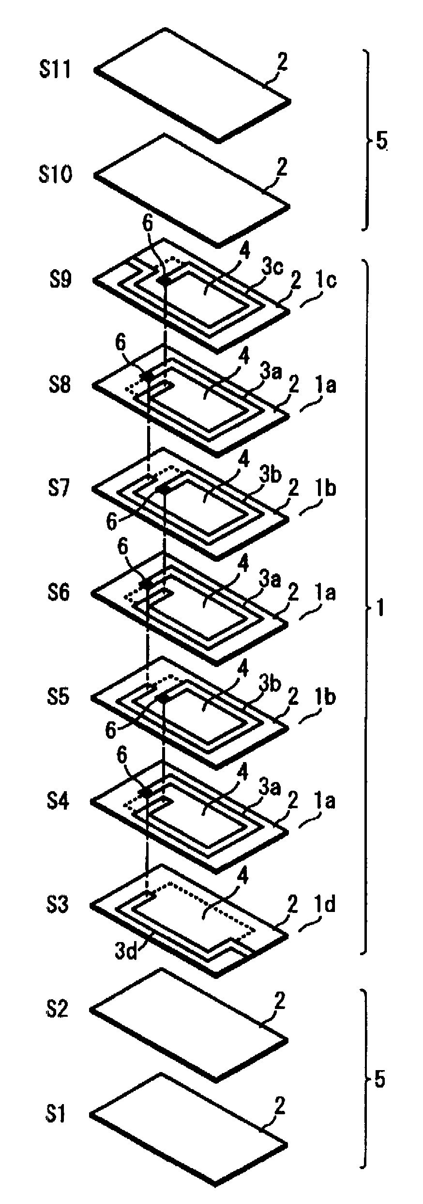
[0124]100 parts by weight of calcined Ni—Cu—Zn ferrite powder (Curie temperature Tc: 240° C., and initial permeability at a frequency of 100 kHz: 300) comprising 49.0% by mol of Fe2O3, 13.0% by mol of CuO, and 21.0% by mol of ZnO, the balance being NiO, was blended with 10 parts by weight of an organic binder based on polyvinyl butyral, a plasticizer and a solvent by a ball mill, to form a magnetic material slurry, which was formed into green sheets.

[0125]Some of the green sheets were provided with through-holes 6, and the green sheets having through-holes 6 and those without through-holes were printed with a non-magnetic zirconia paste for forming magnetic gap layers 4 in a predetermined pattern, and then printed with a conductive Ag paste for forming coil patterns 3.

[0126]To remove a step between the printed zirconia paste layer and the printed Ag paste layer, an imprinted region was printed with a ...

example 2

(1) Production of First Laminate Device Shown in FIGS. 7 and 8 (Sample 4 of Example)

[0131]A laminate device (laminated inductor, Sample 4) of 3.2 mm×1.6 mm and 1.0 mm in thickness having 7-μm-thick magnetic gap layers formed on all of 16 coil-pattern-carrying layers was produced in the same manner as in Example 1, except for using calcined Li—Mn—Zn ferrite powder (Curie temperature Tc: 250° C., and initial permeability at a frequency of 100 kHz: 300) comprising 3.8% by mass of Li2CO3, 7.8% by mass of Mn3O4, 17.6% by mass of ZnO, 69.8% by mass of Fe2O3, and 1.0% by mass of Bi2O3, in place of the calcined Ni—Cu—Zn ferrite powder. To be free from a step, each coil-pattern-carrying layer was printed with a Ni—Zn ferrite paste in a region in which the zirconia paste and the Ag paste were not printed. After sintering, the magnetic substrate layer had a thickness of 40 μm, the coil pattern had a thickness of 20 μm and a width of 300 μm, and a region inside the coil pattern was 2.2 mm×0.6 m...

example 3

Production of Fourth Laminate Device Shown in FIGS. 13 and 14 (Sample 5)

[0137]A laminated inductor (Sample 5) was produced in the same manner as in Sample 4, except that a Li—Mn—Zn ferrite layer was formed in a rectangular opening 14 of 0.3 mm×0.3 mm provided in a region including the center axis of a coil in the magnetic gap layer. The laminated inductor of Sample 5 was measured with respect to DC-superimposed characteristics and DC-DC conversion efficiency. The results are shown in Table 2 and FIG. 42.

[0138]

TABLE 2Number of TurnsNumber ofNumber ofThickness (μm)Total Gapof Coil PatternCoil-Pattern-Magneticof MagneticLengthSampleon Each LayerCarrying LayersGap LayersGap Layer(μm)41161671125116167112Ferrite-Filled Layer inInductance (μH) WithDC-DC ConversionSampleMagnetic Gap LayerNo Current LoadEfficiency (%)4No3.977.55Formed in all layers10.278.6

[0139]The laminated inductor of this Example (Sample 5) exhibited larger inductance than the second laminate device (Sample 4) at low DC c...


PUM

PropertyMeasurementUnit
switching frequencyaaaaaaaaaa
temperatureaaaaaaaaaa
thicknessaaaaaaaaaa

Abstract

The laminate device of the present invention comprises magnetic layers and coil patterns alternately laminated, the coil patterns being connected in a lamination direction to form a coil, and pluralities of magnetic gap layers being disposed in regions in contact with the coil patterns.

Description

CROSS REFERENCE TO RELATED APPLICATION[0001]This application is a National Stage of International Application No. PCT / JP2007 / 051648 filed Jan. 31, 2007, claiming priority based on Japanese Patent Application Nos. 2006-023775, filed Jan. 31, 2006 and 2006-152542, filed May 31, 2006, the contents of all of which are incorporated herein by reference in their entirety.FIELD OF THE INVENTION[0002]The present invention relates to a laminate device having a magnetic circuit constituted by laminating coil patterns and magnetic material layers, particularly to a laminated inductor having non-magnetic or low-permeability magnetic gap layers in a magnetic circuit path, and a module (composite part) having semiconductor devices and other reactance elements mounted on a ferrite substrate having electrodes, etc.BACKGROUND OF THE INVENTION[0003]Various portable electronic equipments (cell phones, portable information terminals PDA, note-type personal computers, portable audio / video players, digita...

Claims


Application Information

Patent Timeline
Patent Type & Authority Patents(United States)
IPC IPC(8): H01F5/00
CPCH01F17/0013Y10T29/4902H01F2017/0066H01F2017/002H01F3/14H01F17/00H01F17/04
Inventor TADA, TOMOYUKIUMENO, TORUMIYOSHI, YASUHARU
Owner HITACHI METALS LTD
Why Eureka
Try Eureka