Organic light-emitting elements of LED with light reflection layers in each spaced on opposite sides of transparent conductive layer

a technology of organic light-emitting elements and conductive layers, which is applied in the manufacture of electrode systems, electric discharge tubes/lamps, and discharge tubes luminescnet screens, etc., can solve the problems of complex process of varying the thickness of transparent electrodes for every different color, needing high driving voltage, and various problems of above described conventional technologies, so as to improve the light extraction efficiency of organic light-emitting elements and process simple

Active Publication Date: 2011-04-12
CANON KK
View PDF17 Cites 16 Cited by
  • Summary
  • Abstract
  • Description
  • Claims
  • Application Information

AI Technical Summary

Benefits of technology

The present invention is designed with respect to the above described circumstances, and provides an organic light-emitting device which can enhance the light extraction efficiency of organic light-emitting elements for emitting lights of respective emission colors, while reducing a step difference between the organic light-emitting elements for emitting lights of the respective emission colors. The present invention also is directed to a process of producing such an organic light-emitting device in a simpler process.
In an organic light-emitting device according to the present invention, the first electrode has a reflection layer and a transparent conductive layer, and changes a stacking order of the reflection layer and the transparent conductive layer corresponding to respective emission colors. By changing the stacking order in the above way, the organic light-emitting device can appropriately use an organic light-emitting element which uses the transparent conductive layer as a layer for adjusting an optical path length for enhancing light extraction efficiency, and an organic light-emitting element which does not use the transparent conductive layer as the layer for adjusting the optical path length.
Accordingly, even in the case of forming the first electrode including an inorganic oxide material such as ITO, the first electrode can be optically optimally designed on a reflective electrode side (on the first electrode side containing the reflection layer) according to the emission color, without requiring a complicated process of patterning and adjusting the thickness of the first electrode by using an etching technique or the like.
The drive voltage of an organic light-emitting element also does not increase, because of not needing to positively change a thickness of a layer which does not originally need to change the thickness according to each emission color (for instance, a charge injection layer, a charge transport layer and the like), for the purpose of adjusting the optical path length on the first electrode side including the reflection layer, when viewed from a light-emitting layer.
Furthermore, the organic light-emitting device can equalize the total thickness of the first electrode with respect to light-emitting elements for emitting lights of a plurality of emission colors. Accordingly, the organic light-emitting device can reduce a step difference on the surface of an organic layer when forming the second electrode or a sealing layer, and can consequently reduce the risk of causing discontinuities at the step.
Thus, the organic light-emitting device according to the present invention can enhance the light extraction efficiency of a light-emitting element for emitting a light of each emission color while inhibiting a layer formed on the organic compound layer from discontinuities at the step difference, without using a complicated production process.

Problems solved by technology

The multicolor organic EL display unit has many organic EL elements having respective light-emitting layers for emitting lights of red, green and blue colors having different emission spectra arranged on a substrate, and therefore the process of varying a thickness of a transparent electrode (such as ITO) for every different color becomes complicated.
However, the above described conventional technologies had various problems to be solved.
H04-328295 and H07-240277 do not sufficiently disclose how the technologies can be applied to each organic light-emitting element, when an organic light-emitting device has many organic light-emitting elements which emit lights of emission colors such as red, green and blue, formed on the same substrate.
Accordingly, various problems appear when the thickness of each organic compound layer for forming the organic light-emitting element is determined for the purpose of optimizing the optical path length.
When the film thicknesses are set as is described above, the organic light-emitting element of emitting a light of a particular color occasionally results in needing high driving voltage.
But, it does not disclose anywhere specifically how to stack the layer.
In addition, Japanese Patent Application Laid-Open Nos. 2005-197011, 2005-093399 and 2005-093401 disclose a technology of changing the thickness of a transparent electrode (ITO and IZO) according to each emission color, which has been considered to be difficult in the technology described by Japanese Patent Application Laid-Open No. 2000-323277.
However, the technology of changing the thickness of the transparent electrode according to the emission color needs a complicated step like the step of etching an IZO layer using a crystallized ITO as an etching stop, or the step of forming a resist on a position corresponding to each emission color and etching ITO.
Particularly, the ITO has transparency, so that it is difficult to confirm an end point of etching by visual inspection.
An optical path length is a product obtained by multiplying the thickness of the transparent electrode (ITO) in which light transmits by the refractive index, so that the transparent electrode needs to be formed in a precise film thickness in order to optically design the optical path length, but the conventional technologies had difficulty in forming the transparent electrode in the precise thickness.
In this case as well, when there is the step, the metal thin film is easily cut (tends to cause discontinuities at the step), which is unpreferable.
However, the thick sealing film has not been desirable, because of lowering the light-transmissive property and needing a longer period of time in a production process.

Method used


Image

  • Organic light-emitting elements of LED with light reflection layers in each spaced on opposite sides of transparent conductive layer
  • Organic light-emitting elements of LED with light reflection layers in each spaced on opposite sides of transparent conductive layer
  • Organic light-emitting elements of LED with light reflection layers in each spaced on opposite sides of transparent conductive layer

Examples


first embodiment

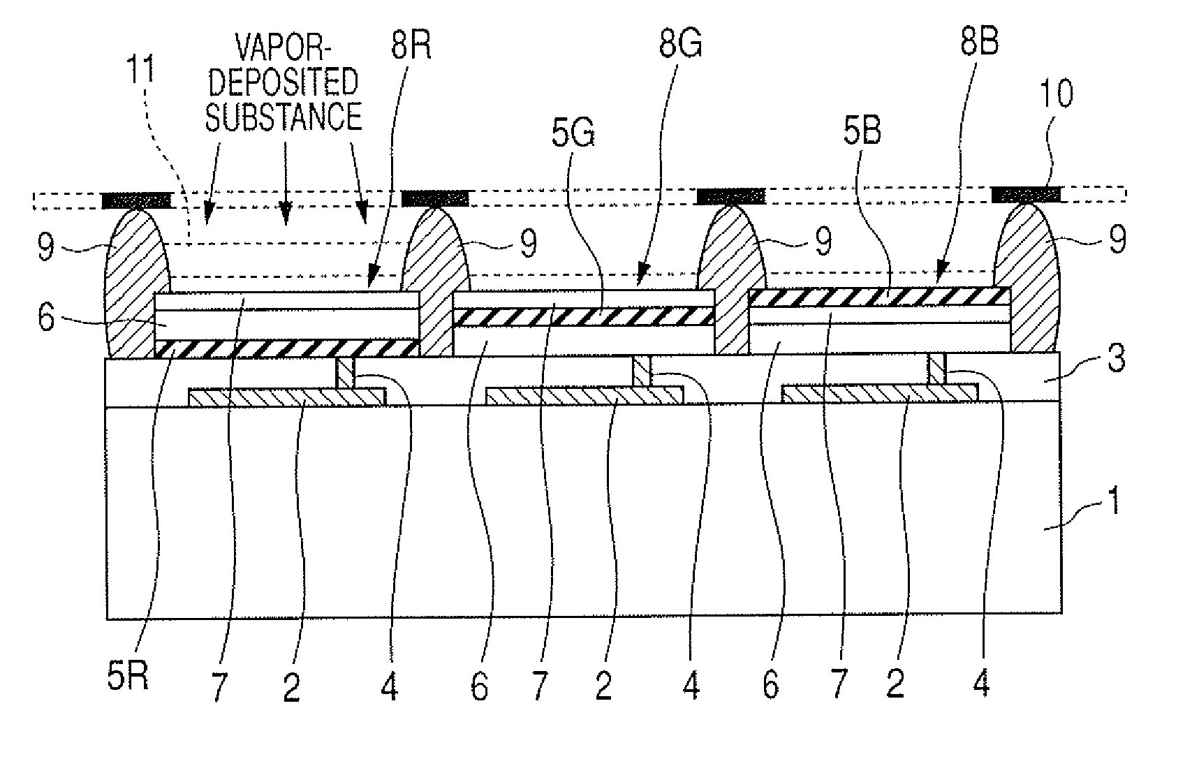
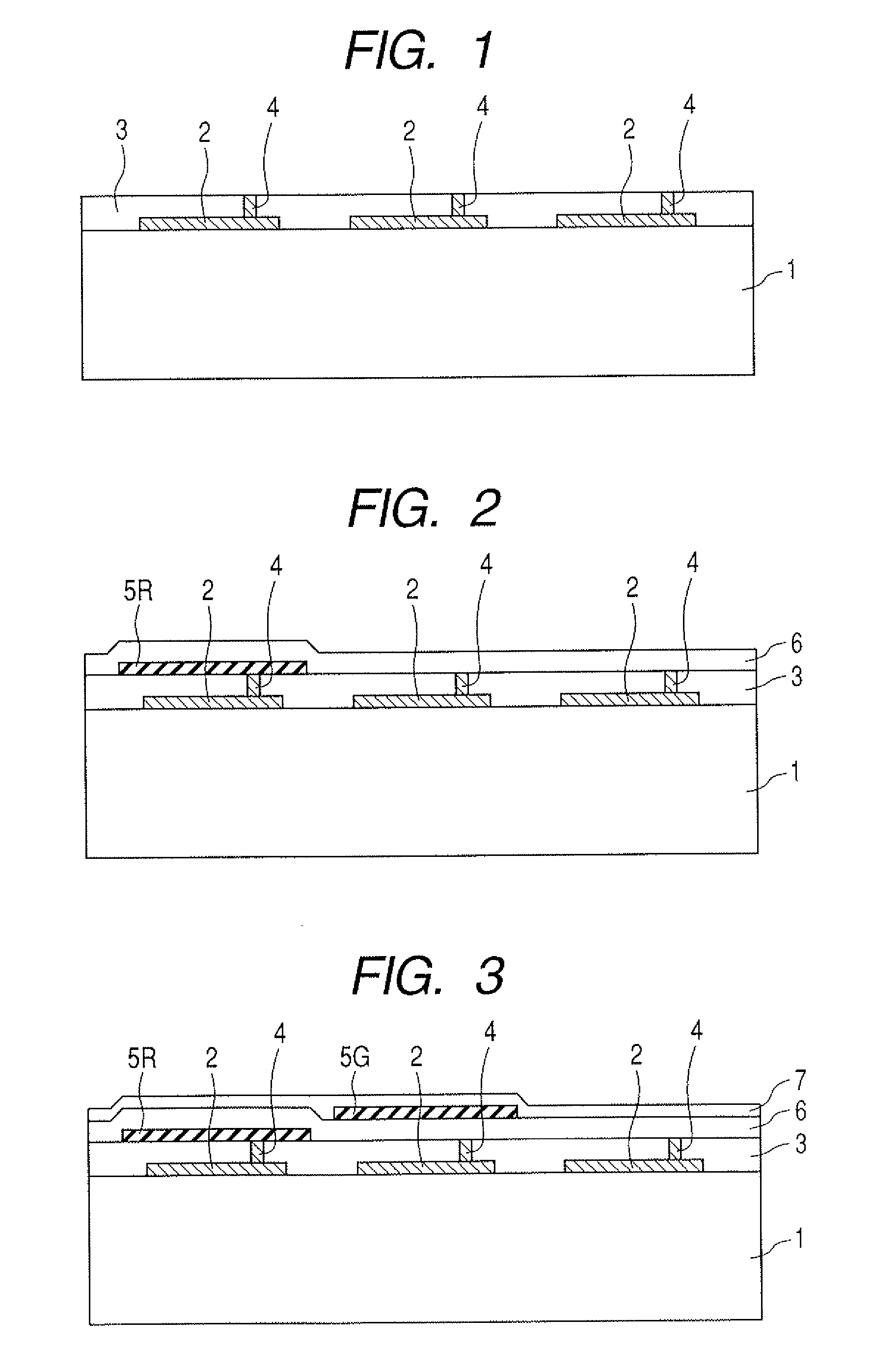
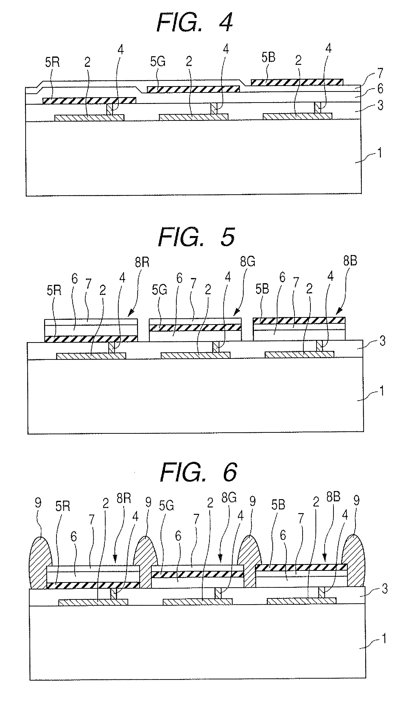
FIG. 1 to FIG. 9 are schematically sectional views showing the sequential steps of a process of producing an organic light-emitting device according to a first embodiment of the present invention.

The organic light-emitting device according to the first embodiment of the present invention has organic light-emitting elements which can emit the lights of three colors (three primary colors) of red, green and blue respectively formed on a substrate. However, such an organic light-emitting device can be also produced in a similar production process to that of the above organic light-emitting device, as is further provided with an organic light-emitting element which can further emit another color like a white color, in addition to the three primary colors of red, green and blue. Each organic light-emitting element in the organic light-emitting device is a top-emission element which emits the light emitted from a light-emitting layer in a direction opposite to the substrate.

An organic ligh...

second embodiment

FIG. 10 is a schematic view showing a diagrammatic structure on the way of a process of producing an organic light-emitting device according to a second embodiment of the present invention. In addition, FIG. 10 relating to the second embodiment corresponds to FIG. 5 relating to a first embodiment.

As is shown in FIG. 10, the organic light-emitting device according to the second embodiment has an ITO film (third transparent conductive layer 14) stacked on the outermost surfaces (light-extracting side) of the first electrodes 8R, 8G and 8B of organic light-emitting elements for respective colors, which is a different point from the organic light-emitting device according to the first embodiment (see FIG. 5).

That is, on the reflection layer 5B for a blue light-emitting element in the first embodiment, further a third transparent conductive layer 14 made of vapor-deposited ITO having a thickness of 10 nm is formed to become the first electrode 8B for blue in the present embodiment. In ad...

third embodiment

FIG. 11 is a schematic view showing a diagrammatic structure of an organic light-emitting device according to a third embodiment of the present invention. In addition, FIG. 11 relating to the third embodiment corresponds to FIG. 9 relating to a first embodiment.

As is shown in FIG. 11, the organic light-emitting device according to the third embodiment has a semi-transparent reflection layer 15 provided the lowest surface (opposite side of a light-extracting side) of a second electrode 12 of an organic light-emitting element for each color, which is a different point from an organic light-emitting device according to the first embodiment (see FIG. 9). The semi-transparent reflection layer 15 is made of a conductive material and constitutes the second electrode in the present embodiment. Except the above point, the organic light-emitting device according to the third embodiment has an approximately similar structure to that of the organic light-emitting device according to the first e...


PUM


Abstract

An organic light-emitting device has a substrate and a plurality of organic light-emitting elements formed on the substrate. The plurality of the organic light-emitting elements include a first light-emitting element emitting light of a first emission color, and a second light-emitting element emitting light of a different emission color. Each light-emitting element has, in sequence, a first electrode having a light reflection layer and a transparent conductive layer, an organic compound layer containing a light-emitting layer, and a second electrode on the substrate. The light reflection layer of the first element is between the substrate and the transparent conductive layer and the light reflection layer of the second element is between the transparent conductive layer and the organic compound layer. A thickness of the transparent conductive layer of the first and second organic light-emitting elements is the same.

Description

BACKGROUND OF THE INVENTION1. Field of the InventionThe present invention relates to an organic light-emitting device including an organic light-emitting element which emits light when an electric current is applied to an organic compound layer containing a light-emitting layer which is formed between a pair of electrodes, and a method for producing the same. Particularly, the present invention relates to an organic light-emitting device including an organic light-emitting element which can emit light of a plurality of colors, and a method for producing the same.2. Description of the Related ArtConventionally, an electroluminescence (EL) element and a light-emitting diode (LED) have been known as a self-luminous element for use in a display unit or a light source. Among them, an organic light-emitting element (hereinafter may be referred to as organic EL element or the element) including an organic compound material for a light-emitting layer has received attention, because the elem...

Claims


Application Information

Patent Timeline
Patent Type & Authority Patents(United States)
IPC IPC(8): H05B33/00H01L51/50H01J1/63
CPCH01L51/5271H01L51/5265H01L27/3246H10K59/122H10K50/852H10K50/856
Inventor NAKAMURA, NAOTO
Owner CANON KK
Why Eureka
Try Eureka