Apparatus and method for detecting terahertz wave

a technology of terahertz light and apparatus, applied in the field of apparatus and method for detecting terahertz light, can solve the problems of inability to apply existing techniques, such as optics and electronics, to achieve the effect of wide frequency range, clear detection, and accurate measurement of terahertz light frequency

Inactive Publication Date: 2011-05-24
RIKEN
View PDF3 Cites 15 Cited by
  • Summary
  • Abstract
  • Description
  • Claims
  • Application Information

AI Technical Summary

Benefits of technology

[0032]The present invention has been made to solve the above-mentioned problems. It is an object of the present invention to provide a terahertz wave detecting apparatus and its method, capable of clearly detecting the intensity of very weak terahertz light in a small-scale apparatus structure using unique electronic properties of graphene without the need for ultralow temperatures, and capable of accurately measuring the frequency of the terahertz light in a very wide frequency range.
[0063]Further, since the ability of graphene electrons to conduct current is more than 10 to 100 times that of normal semiconductor materials such as silicon at room temperature, the intensity of very weak terahertz light can be detected clearly without the need for ultralow temperatures. In addition, the frequency can be measured accurately in a very wide frequency range.
[0064]To sum up, the present invention has the following advantages:
[0066](2) Because the ability of electrons to conduct current is high, the need for ultralow temperatures is eliminated and very weak terahertz light can be detected.

Problems solved by technology

However, since the terahertz light is electromagnetic waves the frequency band of which is interposed between light (5×10¹³ to 1015 Hz in frequency), such as near-infrared rays, visible light, and ultraviolet rays, and radio waves (103 to 1012 Hz in frequency), there is a problem that existing techniques, such as optics and electronics, cannot be applied as they are.
Therefore, the carbon nanotubes cannot be placed in desired positions with respect to the impurities during manufacturing of the detector.
Further, since sharp wavelength selectivity is not provided at the impurity level, the frequency of terahertz light cannot be measured.
The terahertz light detector disclosed in Non-Patent Document 2 requires ultralow temperatures of 0.3 to 0.4 K to obtain high sensitivity, and hence it requires use of an expensive, large-scale helium-3 cryostat.
The conventional terahertz light detectors further have a problem that the frequency range of detectable terahertz light is narrow.

Method used


Image

  • Apparatus and method for detecting terahertz wave
  • Apparatus and method for detecting terahertz wave
  • Apparatus and method for detecting terahertz wave

Examples


first embodiment

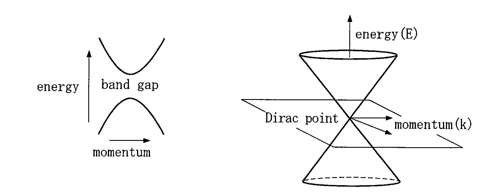
[0132]In a single layer of graphene, since the carriers are Dirac fermions, the formation of Landau levels due to the magnetic field is greatly different from that in normal semiconductor materials in that the level spacing spans a considerably wide band from far-infrared to mid-infrared (between about 1 to 50 THz). Therefore, the exploration of the unique Landau level structure and the application thereof to the implementation of frequency-tunable terahertz detectors can be expected. Thus, the electron transport properties of graphene under the interaction with terahertz waves have been examined.

[0133]FIG. 9A and FIG. 9B are graphs showing first experimental results of the dependence of changes in electrical resistance on the magnetic field with respect to the irradiation of terahertz waves (at a temperature of 4.2K). FIG. 9A shows the result on graphene two-dimensional electron gas (2DEG), and FIG. 9B shows the result on normal GaAs / AlGaAs-2DEG. In this experiment, terahertz waves...

second embodiment

[0137]FIG. 10A and FIG. 10B are graphs showing second experimental results similar to those of the first embodiment. In this second embodiment, terahertz waves at a wavelength of 70.6 μm (where the photon energy is 17.6 meV and the frequency is 4.2 THz) were used.

[0138]It is apparent from FIG. 10B that any response signal (peak) indicative of absorption of electromagnetic waves was not observed in the GaAs-2DEG. If the effective mass of GaAs is assumed to be 0.067 m0 like in the first embodiment, the inter-Landau-level energies of the GaAs-2DEG are 0 to 8.5 meV. Since the photon energy (17.6 meV) of the irradiated terahertz waves is larger than the inter-Landau-level energy spacing of the GaAs-2DEG, it can be said that the result that no peak indicative of absorption of electromagnetic waves was not observed is reasonable.

[0139]In contrast, in the graphene 2DEG of FIG. 10A, a clear peak appears at 1.29 T. The static magnetic field when electromagnetic waves of 17.6 meV are absorbed ...

third embodiment

[0141]FIG. 11A and FIG. 11B are graphs showing third experimental results similar to those of the first embodiment. In this third embodiment, terahertz waves at a wavelength of 184 μm (where the photon energy is 6.7 meV and the frequency is 1.6 THz) were used.

[0142]It is apparent from FIG. 11B that a response signal (peak) indicative of absorption of electromagnetic waves in the GaAs-2DEG was observed in this example. If the effective mass of GaAs is assumed to be 0.067 m0 like in the first embodiment, the inter-Landau-level energy spacing of the GaAs-2DEG are 0 to 8.5 meV. On the other hand, since the photon energy (6.7 meV) of the irradiated terahertz waves falls within the above-mentioned range of inter-Landau-level energies, it can be said that the result that the peak indicative of absorption of electromagnetic waves was observed is reasonable.

[0143]In contrast, in the graphene 2DEG of FIG. 11A, a peak appears at 0.19 T. The static magnetic field when electromagnetic waves of 6...


PUM


Abstract

A terahertz wave detecting apparatus includes a semiconductor chip 12, a two-dimensional graphene 14, a conductive source electrode 15, and a drain electrode 16 and a gate electrode 17. The two-dimensional graphene 14 is connected to the source electrode and the drain electrode. The apparatus further includes a SD voltage detection circuit 18, a gate voltage applying circuit 19 and a magnetic field generating device 20.

Description

[0001]This application claims priority from Japanese Patent Application No. 2009-027537 filed Feb. 9, 2009, the entire disclosure of which is incorporated herein by reference.BACKGROUND OF THE INVENTION[0002]1. Field of the Invention[0003]The present invention relates to an apparatus and a method for detecting the intensity and frequency of weak terahertz waves.[0004]2. Description of the Related Art[0005]In the present invention, the term “terahertz waves” means electromagnetic waves whose frequency is in the range of 1 to 50 THz (where, 1 THz=1012 Hz), i.e., whose wavelength is in the range from a 0.006-0.3 mm, corresponding to or belonging to submillimeter-wave region to the far-infrared region. In the following description, the “terahertz waves” are referred to as “terahertz light.”[0006]The terahertz light is expected to be applied in a wide range of fields, ranging from basic science fields such as radio astronomy, materials science, and bimolecular spectroscopy to practical f...

Claims


Application Information

Patent Timeline
Patent Type & Authority Patents(United States)
IPC IPC(8): G01J5/02
CPCH01L31/09H01L31/028Y02E10/547
Inventor KAWANO, YUKIOISHIBASHI, KOJI
Owner RIKEN
Why Eureka
Try Eureka