Manufacturing method for epitaxial wafer

a manufacturing method and technology for epitaxial wafers, applied in vacuum evaporation coatings, spraying apparatuses, coatings, etc., can solve problems such as difficult correction, pattern displacement in random orientation, and distortion on the back surface of semiconductor wafers, so as to prevent the decrease in the flatness of the epitaxial wafers, the effect of reducing distortion

Active Publication Date: 2011-06-14
SUMCO CORP
View PDF5 Cites 10 Cited by
  • Summary
  • Abstract
  • Description
  • Claims
  • Application Information

AI Technical Summary

Benefits of technology

[0015]The present inventors have conducted an intensive research and found that the abovementioned problems can be solved by providing a semiconductor oxide film on an entire back surface of a semiconductor wafer that is to be epitaxially grown, and then partially removing the oxide film in a round shape that is concentric with the semiconductor wafer, in other words, by leaving the semiconductor oxide film in an outer peripheral portion where sticking with the susceptor is likely to occur and removing the semiconductor oxide film in a site that is positioned above the lift pin when housed at a wafer placement portion.
[0020]According to the present invention, there is provided a manufacturing method for an epitaxial wafer that can alleviate distortions on a back surface thereof due to sticking between a wafer and a susceptor, thereby preventing decrease in flatness of the epitaxial wafer due to a lift pin being present.

Problems solved by technology

Furthermore, if such sticking occurs between the back surface of the semiconductor wafer and the susceptor, distortions on the back surface of the semiconductor wafer may be generated due to difference in thermal expansion between the semiconductor wafer and the susceptor when temperature of the heater rises and falls and when the heater is in a high temperature state.
Such distortions may lead to pattern displacement in a random orientation, which is difficult to correct, in thermal processing before the photolithography processing of the semiconductor wafer, in a production process of a semiconductor device.
There has been a problem in that such pattern displacement further leads to misalignment in photolithography processing.
However, Japanese Unexamined Patent Application Publication No. 2006-5164 discloses only a method for evaluating the surface configuration of an epitaxial wafer and does not disclose a concrete method for alleviating distortions on a back surface of the epitaxial wafer.
However, the lift pin is generally formed of a material having a thermal conductivity different from that of the susceptor, leading to a nonuniform temperature distribution on a surface of a wafer placed on the susceptor.
Therefore, such an epitaxial wafer, of which flatness is low in parts thereof, is a factor contributing to a lower yield in manufacturing of semiconductor devices.

Method used


Image

  • Manufacturing method for epitaxial wafer
  • Manufacturing method for epitaxial wafer
  • Manufacturing method for epitaxial wafer

Examples


example 1

[0079]A p-type silicon wafer of 300 mm in diameter, which is double-side polished, was set on a single wafer processing cleaner. First, as the oxide film forming step, ozone water solution (20 ppm in concentration) was sprayed onto a main surface and a back surface of the silicon wafer at a feed rate of 1 SLM for 1 minute while rotating the silicon wafer at 1000 rpm, thereby forming an oxide film on the main surface and the back surface thereof. Next, as the etching step, hydrofluoric acid water solution (1% by mass in concentration) was sprayed onto the back surface at a feed rate of 1 SLM for 1 minute while rotating the silicon wafer at 10 rpm, thereby removing the oxide film formed on the back surface of the silicon wafer except for in an outer peripheral portion thereof. Thereafter, the main surface and the back surface of the silicon wafer were cleaned by spraying pure water thereonto. Spray nozzles of the ozone water solution and the hydrofluoric acid water solution were dispo...

example 2

[0084]The oxide film forming step and the etching step were performed in the same conditions except for conditions of the etching step, where rotating speed of the silicon wafer being 30 rpm and spraying time of the hydrofluoric acid water solution being 1 minute.

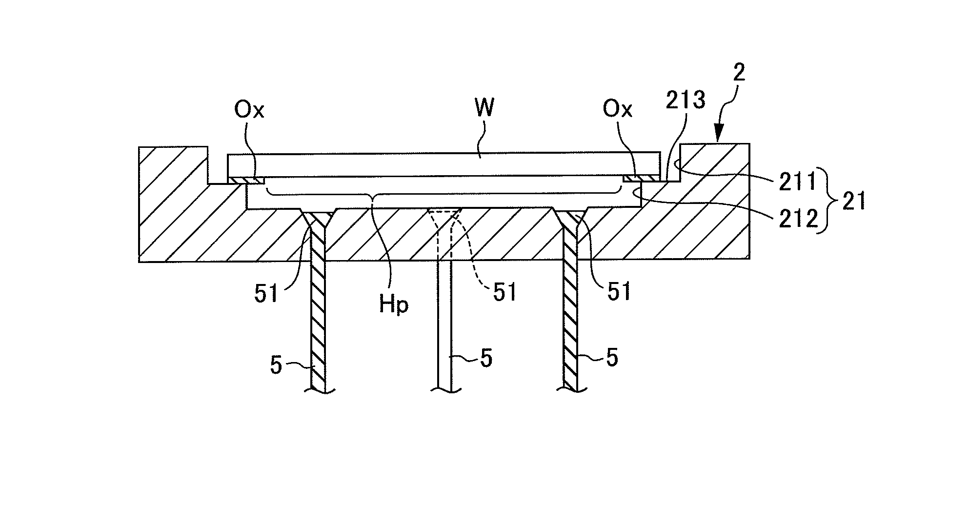
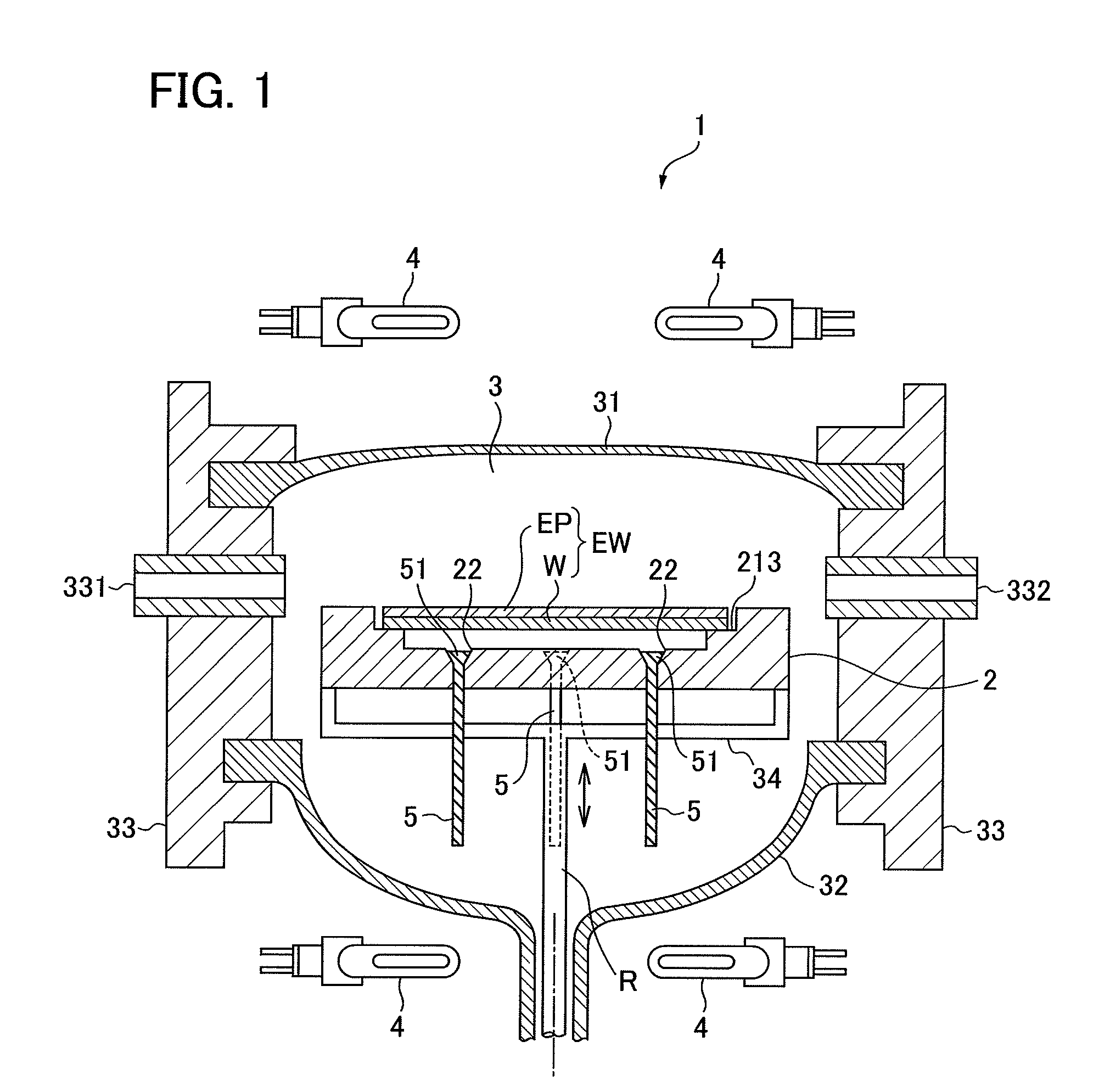
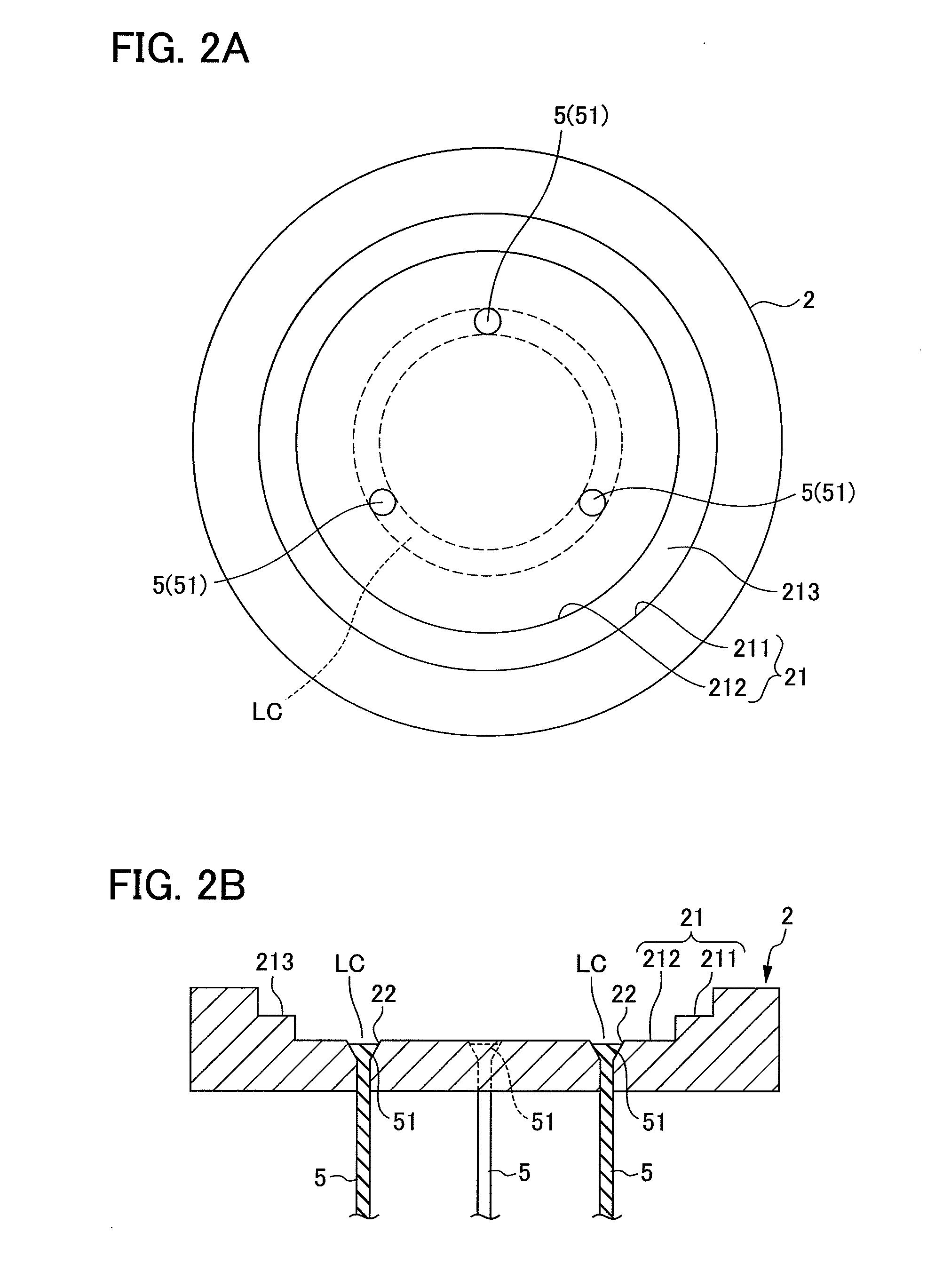
[0085]In the abovementioned process, the oxide film on the back surface of the silicon wafer was removed except for in a region from 145 to 150 mm away from a center of the silicon wafer (in other words, a region of 5 mm from an outer periphery of the silicon wafer). The water contact angle of a portion where the oxide film remained (a portion 148 mm away from the center) was no greater than 10° and the water contact angle of a portion where the oxide film was removed (a portion 114 mm away from the center, where a lift pin on the susceptor was present) was 40°.

[0086]The silicon wafer thus obtained was epitaxially grown in the same condition as that in Example 1, and distortions in the outer peripheral portion thereof and f...


PUM

PropertyMeasurementUnit
water contact angleaaaaaaaaaa
temperatureaaaaaaaaaa

Abstract

To provide a manufacturing method for an epitaxial wafer that alleviates distortions on a back surface thereof due to sticking between a wafer and a susceptor, thereby preventing decrease in flatness thereof due to a lift pin. A manufacturing method for an epitaxial wafer according to the present invention includes: an oxide film forming step in which an oxide film is formed on a back surface thereof; an etching step in which a hydrophobic portion exposing a back surface of the semiconductor wafer is provided by partially removing the oxide film; a wafer placing step in which the semiconductor wafer is placed; and an epitaxial growth step in which an epitaxial layer is grown on a main surface of the semiconductor wafer; and the diameter of the lift pin installation circle provided on a circle on a bottom face of a susceptor is smaller than that of the hydrophobic portion.

Description

[0001]This application is based on and claims the benefit of priority from Japanese Patent Application No. 2008-327274, filed on 24 Dec. 2008, the content of which is incorporated herein by reference.BACKGROUND OF THE INVENTION[0002]1. Field of the Invention[0003]The present invention relates to a manufacturing method for an epitaxial wafer using a vapor phase growth system.[0004]2. Related Art[0005]An epitaxial wafer is a semiconductor wafer in which an epitaxial layer is grown on a main surface thereof. Recently, there is a demand for epitaxial wafers having high flatness and high definition is required accompanying increased integration of semiconductor devices and design rule miniaturization (miniaturized pattern). A vapor phase growth system that grows an epitaxial layer on a main surface of a semiconductor wafer is used for manufacturing an epitaxial wafer.[0006]With the vapor phase growth system, an epitaxial layer can be grown on a main surface of a semiconductor wafer accor...

Claims


Application Information

Patent Timeline
Patent Type & Authority Patents(United States)
IPC IPC(8): H01L21/20C23C16/00
CPCC23C16/4411C23C16/481H01L21/68742C23C24/082H01L21/02532H01L21/02579
Inventor WADA, NAOYUKITAKEMURA, MAKOTO
Owner SUMCO CORP
Why Eureka
Try Eureka