Methods for manufacturing MEMS sensor and thin film and cantilever beam thereof with epitaxial growth process

a technology of epitaxial growth and manufacturing method, which is applied in the direction of fluid pressure measurement, fluid pressure measurement by electric/magnetic elements, instruments, etc., can solve the problems of not being able to uniformly thickness inside and outside pressure-sensitive silicon films, not being able to manufacture pressure-sensitive silicon films of piezoresistive pressure sensors,

Active Publication Date: 2011-07-05
MEMSENSING MICROSYST SUZHOU CHINA
View PDF2 Cites 23 Cited by
  • Summary
  • Abstract
  • Description
  • Claims
  • Application Information

AI Technical Summary

Benefits of technology

[0056]Besides, the single-crystal silicon film 106 cannot be etched in the following etching processes as a result that the thickness of the single-crystal silicon film 106 can be well controlled. The traditional etching process with the silicon wafer etched from its bottom surface can't prevent the diaphragm from further being etched. As a result, the thickness of the diaphragm can't be well controlled. However, the current fabrication method of the first embodiment of the present invention can overcome such difficulty of the traditional method. Besides, the current fabrication method is simple and useful because no additional apparatus, such as the expensive potentiostats or clip tools for protecting the silicon wafer, is needed.

Problems solved by technology

However, such method is not suitable to fabricate a single-crystal silicon film.
However, such method cannot uniform the thickness of the inside and outside pressure-sensitive silicon films.
However, since the piezoresistances cannot be fabricated on the highly doped silicon film, such method is not suitable to manufacture the pressure-sensitive silicon films of the piezoresistive pressure sensors.
However, such method needs additional apparatus, such as expensive potentiostats and clip tools for protecting the silicon wafer.
Usually, the cantilever beam is fabricated from a single-crystal silicon film, which still meets the problems described in the above piezoresistive pressure sensors.

Method used


Image

  • Methods for manufacturing MEMS sensor and thin film and cantilever beam thereof with epitaxial growth process
  • Methods for manufacturing MEMS sensor and thin film and cantilever beam thereof with epitaxial growth process
  • Methods for manufacturing MEMS sensor and thin film and cantilever beam thereof with epitaxial growth process

Examples


first embodiment

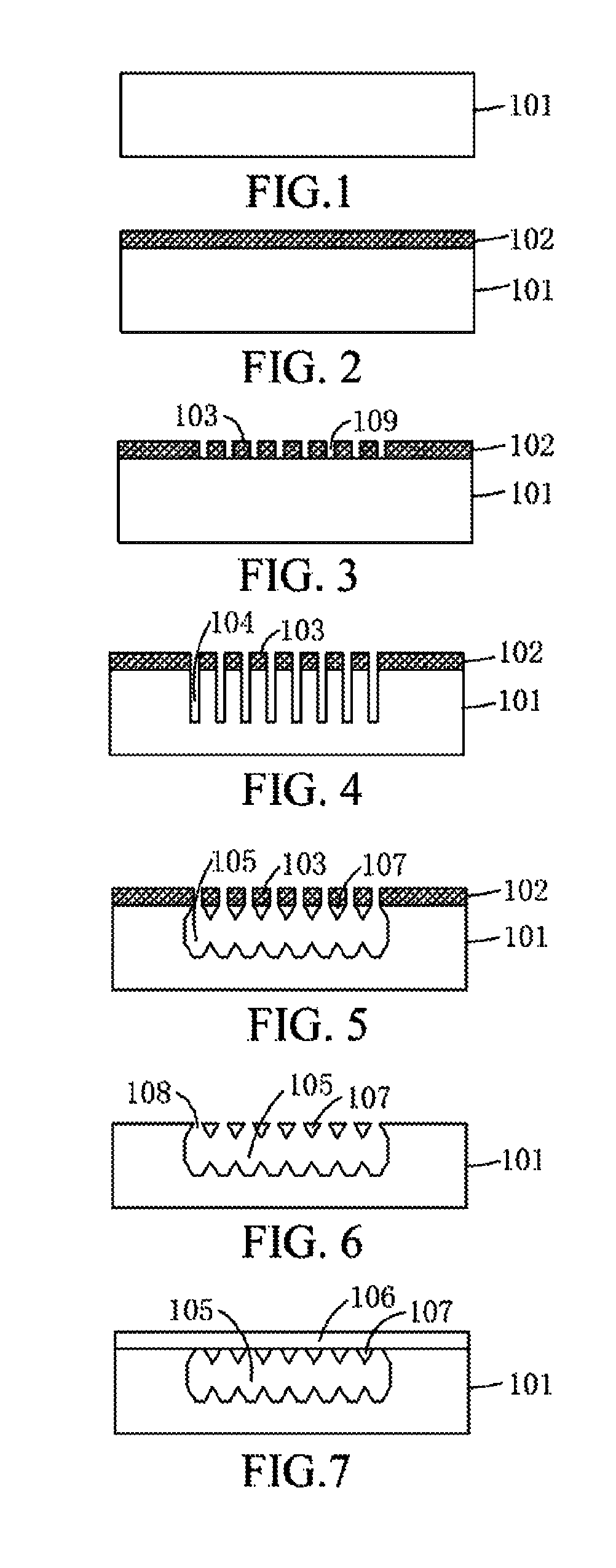
[0049]Please refer to FIGS. 1-7, a method for fabricating a thin film of a MEMS sensor according to the present invention is disclosed and includes the following steps.

[0050]Please refer to FIGS. 1 and 2, firstly, a medium layer 102 is formed on a top surface of a single-crystal silicon wafer 101 via a deposition process, such as a Low Pressure Chemical Vapor Deposition (LPCVD) process or a Plasma Enhanced Chemical Vapor Deposition (PEVCD) process or a thermal oxidation process. The medium layer 102 is made of silicon oxide or silicon nitride to function as a mask layer in the following etching processes.

[0051]Secondly, referring to FIG. 3, the medium layer 102 is partly removed via an etching process, such as a photo etching process or a dry etching process or a wet etching process, in order to form a meshwork mask diagram 103.

[0052]Thirdly, referring to FIG. 4, a plurality of trenches 104 are formed by etching the single-crystal silicon wafer 101 through the mask diagram 103 via a...

second embodiment

[0057]Please refer to FIGS. 10-16, a method for fabricating a mass block of a MEMS sensor according to the present invention is disclosed and includes the following steps.

[0058]Please refer to FIGS. 10 and 11, firstly, a top surface of a single-crystal silicon wafer 201 is etched via an etching process, such as a photo etching process or a dry etching process or a wet etching process, in order to form a deep hole 202. The deep hole 202 further extends into an inner side of the single-crystal silicon wafer 201.

[0059]Secondly, referring to FIG. 12, a medium layer 203 is then formed on the top surface of the single-crystal silicon wafer 201 via a deposition process, such as a Low Pressure Chemical Vapor Deposition (LPCVD) process or a Plasma Enhanced Chemical Vapor Deposition (PEVCD) process or a thermal oxidation process. The medium layer 203 is made of silicon oxide or silicon nitride and fills in the deep hole 202 to form a sacrificial layer 207.

[0060]Thirdly, referring to FIG. 13, ...

third embodiment

[0065]Please refer to FIGS. 17-27, a method for fabricating a cantilever beam of a MEMS sensor according to the present invention is disclosed and includes the following steps.

[0066]Please refer to FIGS. 17 and 18, firstly, a top surface of a single-crystal silicon wafer 201 is etched via an etching process, such as a photo etching process or a dry etching process or a wet etching process, in order to form a deep hole 202. The deep hole 202 further extends into an inner side of the single-crystal silicon wafer 201.

[0067]Secondly, referring to FIG. 19, a medium layer 203 is then formed on the top surface of the single-crystal silicon wafer 201 via a deposition process, such as a Low Pressure Chemical Vapor Deposition (LPCVD) process or a Plasma Enhanced Chemical Vapor Deposition (PEVCD) process or a thermal oxidation process. The medium layer 203 is made of silicon oxide or silicon nitride and fills in the deep hole 202 to form a sacrificial layer 207. The medium layer 203 functions ...


PUM


Abstract

A method for manufacturing a MEMS sensor and its thin film and cantilever beam includes steps of etching a top surface of a single-crystal silicon wafer in combination of a deposition process, an outer epitaxial growth process, a wet etching process and a back etching process in order to form a pressure-sensitive single-crystal silicon film, a cantilever beam, a mass block, a front chamber, a back chamber and trenches connecting the front and the back chambers. The single-crystal silicon film is prevented from etching so that the thickness thereof can be well controlled. The method of the present invention can be used to replace the traditional method which forms the back chamber and the pressure-sensitive single-crystal silicon film from the bottom surface of the silicon wafer.

Description

BACKGROUND OF THE INVENTION[0001]1. Field of the Invention[0002]The present invention relates to a method for manufacturing a MEMS sensor and methods for fabricating a thin film and a cantilever beam of such MEMS sensor with epitaxial growth processes.[0003]2. Description of Related Art[0004]Micro-Electro-Mechanical Systems (MEMS) is a high technology rapidly developed in recent years. MEMS components can be manufactured by advanced semiconductor manufacturing processes to realize mass production. Compared with the traditional electronic components, the MEMS components are more competitive in profile, power consumption, weight and price etc.[0005]Usually, a MEMS condenser includes micro structures such as a thin film, a mass block and a cantilever beam etc. The traditional method for manufacturing such thin film uses surface sacrificial processes which include steps of: (i) fabricating a sacrificial layer by a Low Pressure Chemical Vapor Deposition (LPCVD) process or a Plasma Enhanc...

Claims


Application Information

Patent Timeline
Patent Type & Authority Patents(United States)
IPC IPC(8): H01L21/00
CPCB81C1/00182G01L9/0042G01P15/0802G01P15/123B81B2201/0235B81B2201/0264B81B2203/0118B81B2203/0315B81B2203/0376B81C2201/0132B81C2201/0177B81C2203/0118G01P2015/0828
Inventor LI, GANGHU, WEI
Owner MEMSENSING MICROSYST SUZHOU CHINA
Why Eureka
Try Eureka