Surface-emission type semiconductor laser

a semiconductor laser and surface emission technology, applied in semiconductor lasers, laser details, electrical equipment, etc., can solve the problems of affecting the overall performance of the system, so as to reduce the effective optical path length, shorten the leff, and improve the effect of pulse frequency

Inactive Publication Date: 2011-07-05
NEC CORP
View PDF13 Cites 1 Cited by
  • Summary
  • Abstract
  • Description
  • Claims
  • Application Information

AI Technical Summary

Benefits of technology

[0113]In the surface-emission type semiconductor laser according to the present invention, such a structure is selected in which the laser comprises a dielectric DBR and on the opposite side thereof, a semiconductor DBR, as an upper DBR and lower DBR to be employed for the construction of a vertical cavity. Further, regarding the resonator part made up of a semiconductor sandwiched by the dielectric DBR and semiconductor DBR, relative to the lasing wavelength λ0, in the case when the optical path length L of the resonator part made up of the semiconductor is selected such that 0.9×λ0≦L≦1.1×λ0, the materials, which are respectively used to make up the dielectric DBR, the semiconductor DBR, and the resonator part made up of the semiconductor, are selected according to the condition defined by equations (1) and (2), as described above. Alternatively, in the case when the optical path length L of the resonator part is selected such that 1.4×λ0≦L≦1.6×λ0, the materials, which are respectively used to make up the dielectric DBR, the semiconductor DBR, and the resonator part made up of the semiconductor, are selected according to the condition defined by equations (3) and (4), as described above. As the component (LDBReff2+LDBReff1) that are caused by the penetration depth of light into the upper DBR and lower DBR is reduced by such choices, the reduction of the effective optical path length: Leff=L+(LDBReff2+LDBReff1) of the resonator is achieved. As a result, in the surface-emission type semiconductor laser according to the present invention, it is possible to realize a further short Leff can be achieved, in comparison with a structure having a shortest effective cavity length: Left among conventional structures which employed a couple of semiconductor DBR for both upper and lower DBRs, that is, a surface-emission type semiconductor laser comprising a half-wavelength micro-cavity in which the optical path length L of the resonator part sandwiched by the DBRs is selected such that L≈λ0 / 2. Accordingly, in the surface-emission type semiconductor laser according to the present invention, it is possible to achieve further increase in the cut-off frequency for modulation, thereby enabling direct modulation at higher pulse frequencies.
[0114]In addition, since the optical path length L of the resonator part made up of the semiconductor is adapted such that L≈2×(λ0 / 2), or L≈3×(λ0 / 2), it is possible to employ a multiple-quantum-well structure as the active layer of the emission region. In such a case, a problem in performing the injection of current into the quantum well, which is inherent to a surface-emission type semiconductor laser which employs a conventional half-wavelength micro-cavity, can be avoided in the surface-emission type semiconductor laser according to the present invention.

Problems solved by technology

On such occasions, improvement in the data transfer speeds between boards and between housings (nodes) for accommodating multiple boards cannot catch up such rapid increases in the data traffic volume to be transferred, which becomes a bottleneck for the improvement in the overall performance of the system.
In the case when a digital signal is transmitted as an electric signal, the loss in a transmission path becomes larger as the frequency increases, and in the case of a high-bit-rate digital signal, distortion takes place in its pulse waveform.
Due to this waveform distortion, in an electric signal transmission, the bit-rate at which data can be transmitted without bit errors is limited.
Further, since crosstalk takes place between transmission lines which are arranged close to each other, it is difficult to arrange transmission lines at high density.

Method used


Image

  • Surface-emission type semiconductor laser
  • Surface-emission type semiconductor laser
  • Surface-emission type semiconductor laser

Examples


first exemplary embodiment

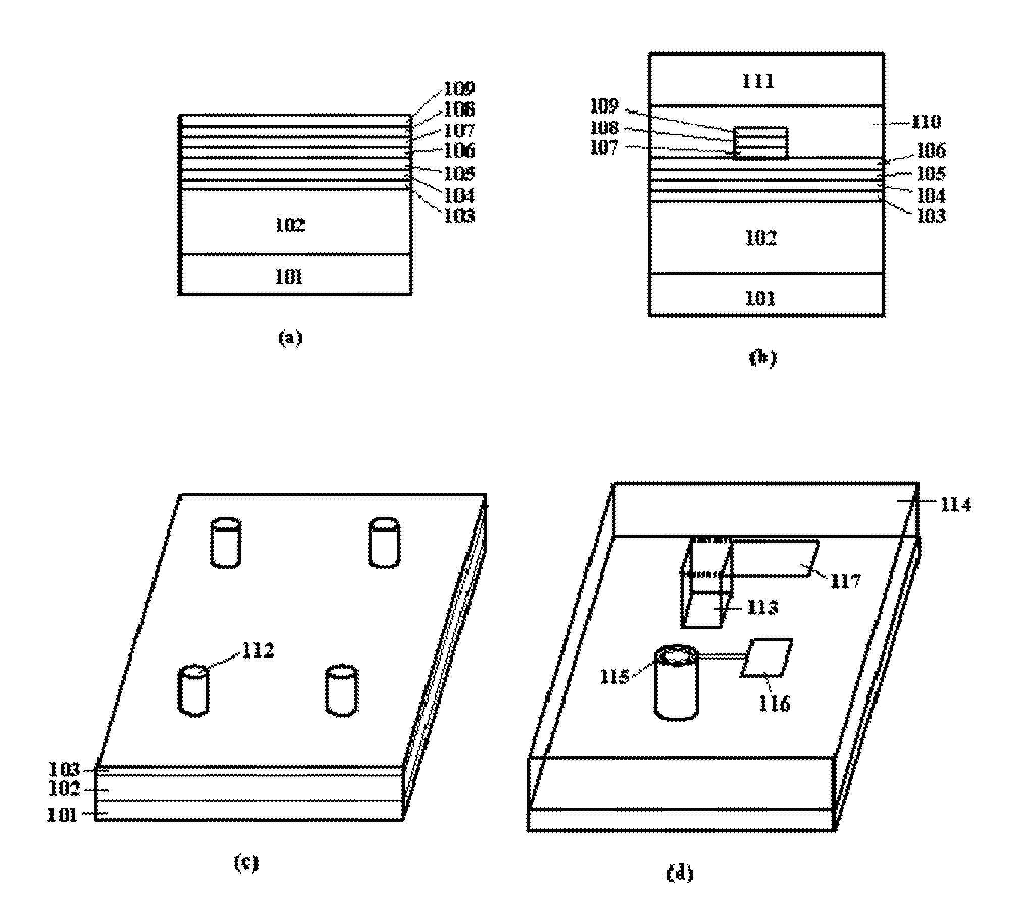
[0194]Hereafter, the structure of the surface-emission type semiconductor laser, device according to a first exemplary embodiment of the present invention will be explained with reference to FIG. 1. This first exemplary embodiment is an example of an application of the present invention to a tunnel-junction type surface-emission laser having a lasing wavelength λ0=1.3 μm, which is formed on a GaAs substrate.

[0195]First, as shown in FIG. 1(a), a first DBR layer 102 which is formed by stacking up plurality of DBRs (n-type semiconductor mirror layer) composed of a pair of an n-type GaAs layer and an n-type AlAs layer as an elementary unit; an n-type GaAs clad layer 103; multiple-quantum-well active layer 104 composed of non-doped GaInNAs well layer and GaAs barrier layer; a p-GaAs clad layer 105; a p-GaAs0.25P0.75 layer 106; a p+-In0.1Ga0.9As layer 107; an n+-Ga0.9In0.1N0.02As0.98 layer 108; and an n-GaAs layer 109 are successively stacked up on an n-type GaAs substrate 101 by a metal-...

second exemplary embodiment

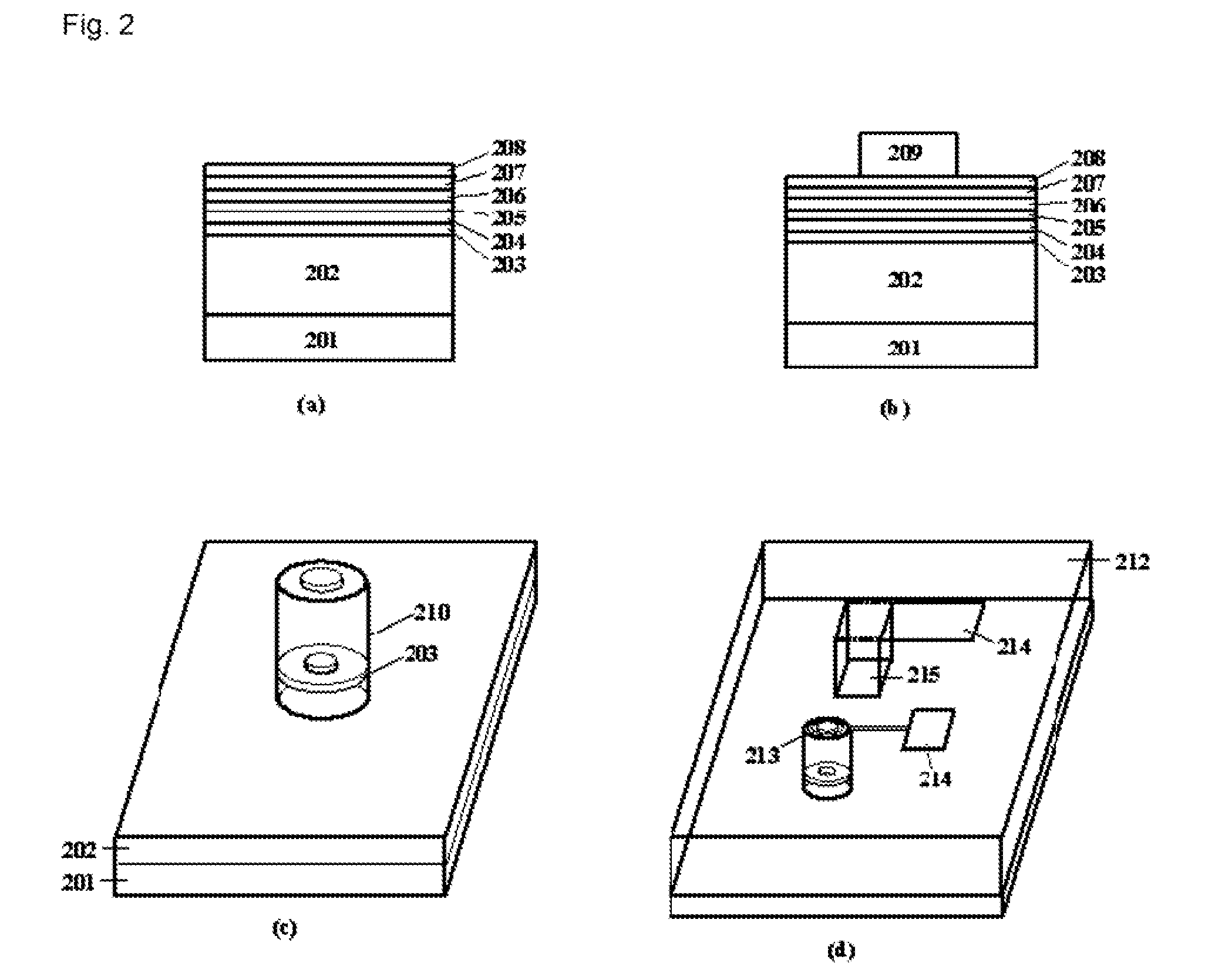
[0214]Hereafter, the structure of a surface-emission type semiconductor laser device according to a second exemplary embodiment of the present invention will be explained with reference to FIG. 2. This second exemplary embodiment is an example of an application of the present invention to a surface-emission type laser of a lasing wavelength λ0=0.85 μm formed on a GaAs substrate.

[0215]First, as shown in FIG. 2(a), a first DBR layer 202 which is formed by stacking up plurality of DBRs (p-type semiconductor mirror layer) composed of a pair of a p-type Al0.12Ga0.85As layer and a p-type Al0.9Ga0.1As as an elementary unit; a layer for forming an oxidized current-confining-part 203 of p-type Al0.98Ga0.02As; a p-type Al0.3Ga0.7As clad layer 204; multilayer quantum well active layer 205 composed of a non-doped GaAs well layer and an Al0.12Ga0.8As barrier layer; an n-type Al0.3Ga0.7As clad layer 206; an n-type Al0.12Ga0.85As layer 207; and a thin n-type GaAs layer 208 are successively stacked...

third exemplary embodiment

[0234]Hereafter, the structure of a surface-emission type semiconductor laser device according to a third exemplary embodiment of the present invention will be explained with reference to FIG. 3. This third exemplary embodiment is an example of an application of the present invention to a tunnel-junction-type surface-emission laser of a lasing wavelength λ0=1.0 μm formed on a GaAs substrate.

[0235]First, as shown in FIG. 3(a), a first DBR layer 302 which is formed by stacking up plurality of DBRs (n-type semiconductor mirror layer) composed of a pair of an n-type GaAs layer and an n-type Al0.9Ga0.1As layer as an elementary unit; an n-type GaAs clad layer 303; a multiple-quantum-well active layers 304 composed of a non-doped InGaAs well layer and a GaAs barrier layer; a p-GaAs clad layer 305; a p-Al0.3Ga0.7As layer 306; a p+-GaAs0.94Sb0.06 layer 307; an n+-In0.12Ga0.88As layer 308; and an n-GaAs layer 309 are successively stacked up on a n-type GaAs substrate 301 by a metal-organic ch...


PUM


Abstract

The present invention provides a surface-emission type semiconductor laser wherein an effective length of a cavity is reduced, thereby enabling to realize a higher-speed direct modulation. In the surface-emission type semiconductor laser according to the present invention, when supposing the optical path length (L) of a resonator part relative to a lasing wavelength λ0 to be given as 0.9×λ0≦L≦1.1×λ0, and denoting the refractive indexes of a high refractive index layer and a low refractive index layer of a dielectric DBR by nH1 and nL1; the average refractive index within an optical path length λ0 / 4 in the semiconductor in contact with the dielectric DBR by nS1; and the refractive indexes of the high refractive index layer and the low refractive index layer of a semiconductor DBR by nH2 and nL2, respective materials to be used are selected so as to satisfy the following conditions (1) and (2):nH1>f(nS1)nL12+g(nS1)nL1+h(nS1),  (1)where f(nS1)=0.0266 nS12−0.2407 nS1+0.6347; g(nS1)=−0.0508 nS12+0.4335 nS1−0.0085; and h(nS1)=0.0382 nS12−0.3194 nS1+0.7398, andnH2−nL2>0.4.  (2)

Description

[0001]This application is the National Phase of PCT / JP2008 / 054703, filed Mar. 14, 2008, which claims the priority based on Japanese Patent Application No. 2007-74881 filed on Mar. 22, 2007, of which entirety is incorporated herein by reference.TECHNICAL FIELD[0002]The present invention relates to a surface-emission type semiconductor laser which is usable as a light source in the fields of optical communications and optical interconnections.BACKGROUND ART[0003]Optical communications which utilize a semiconductor laser as the light source have an advantage such that they enable long-distance transmission and large-capacity transmission. Especially, long-distance optical communications which utilize a long-wavelength semiconductor laser suitable for low-loss silica optical fibers have been widely used in trunk-line systems of communications, etc. from an early period. In general, in a transmission system for optical communications which employ optical fibers as the transmission path, ...

Claims


Application Information

Patent Timeline
Patent Type & Authority Patents(United States)
IPC IPC(8): H01S5/00
CPCH01S5/06226H01S5/1039H01S5/18308H01S5/18369H01S5/227H01S5/3095
Inventor SUZUKI, NAOFUMITSUJI, MASAYOSHIANAN, TAKAYOSHIYASHIKI, KENICHIROHATAKEYAMA, HIROSHIFUKATSU, KIMIYOSHIAKAGAWA, TAKESHI
Owner NEC CORP
Why Eureka
Try Eureka