Method of manufacturing a semiconductor device having an organic thin film transistor

a semiconductor device and organic technology, applied in the field of manufacturing a semiconductor device having an organic thin film transistor, can solve the problems of increased manufacturing cost, fluctuation of performance, and difficulty in manufacturing a fine tft by printing method, and achieve the effect of increasing parasitic capacitance and lowering cos

Inactive Publication Date: 2011-08-02
HITACHI LTD
View PDF9 Cites 1 Cited by
  • Summary
  • Abstract
  • Description
  • Claims
  • Application Information

AI Technical Summary

Benefits of technology

[0009]As has been described above, the method of manufacturing the TFT by using a printing technique has a feature capable of lowering the cost. However, in the usual current printing technique, the positional accuracy is at about 20 μm and it is about several μm even when a modern technique is used. Accordingly, it is difficult to manufacture a fine TFT by the printing method. Particularly in a case where positional displacement should occur for a gate electrode (lower electrode) and source / drain electrodes (upper electrode), it results in a problem of increasing the parasitic capacitance or causing fluctuation for the performance in a case of preparing a plurality of TFTs. It is considered that the positional displacement occurs in the inkjet method upon flying of the material jetted out from a nozzle as far as the substrate. In the transfer method, it is considered that this is caused upon transfer of a material from a transfer roll to a substrate.
[0012]Further, a method of using photosensitive a self-assembled monolayer (hereinafter referred to as a photosensitive SAM) as the photosensitive composition has also been studied. The photosensitive SAM has a feature in that a non-exposed portion is water repellent and an exposed portion becomes hydrophilic. By utilizing the feature, an electroconductive material is selectively printed in the hydrophilic portion to form electrodes or interconnections. For the photosensitive SAM, silane coupling agents having perfluoro alkyl groups, silane coupling agents having photosensitive groups of the photosensitive composition typically represented by resist, etc. have been reported. For the photosensitive SAM having the perfluoro group, a reaction of disconnecting the main chain by using a light at a short wavelength of about 200 nm is used for developing the hydrophilicity and since light at a wavelength of 300 nm or less does not permeate in usual flexible substrates, the reaction is not taken place by the rear face exposure using the flexible substrate. Further, since the exposure wavelength can be adjusted by changing the photosensitive groups in the photosensitive SAM having a resist photosensitive group, some substrates can conduct reaction by light that transmits the flexible substrate. However, since rinsing is not conducted or rinsing is conducted by an organic solvent after exposure, it also involves a problem to take a lot of time for attaining a predetermined hydrophilicity and, further, no sufficient hydrophilicity can be obtained. While there is a method of increasing the hydrophilicity by a treatment with an inorganic alkali after the organic rinsing, this increases the number of steps and extremely increases the time to form the device.
[0013]In view of the foregoing problems, an object of the present invention is to provide a method of manufacturing a high performance organic thin film transistor having a fine pattern shape of about 20 μm in a short time by using a printing method and having a lower electrode and an upper electrode which are positioned with a displacement of 1 μm or less are opposed to each other via an insulating film, without using a photomask.
[0015]A typical embodiment of the invention uses a manufacturing method of using a step of forming a source and drain electrode material by utilizing the difference of the water contact angle changed by exposure without using a photomask only for the positioning step between the upper electrode and the lower electrode and forming all other steps by a printing method. A non-transparent gate electrode (lower electrode) is prepared by using a transport substrate and conducting printing and baking on the transparent substrate by using a conductive material. Then, a transparent insulating film, a photosensitive self-assembled monolayer changing the water contact angle by exposure, and a solution for the conductive material as the source and drain electrode material are stacked above the lower electrode successively for a necessary area by a printing method. Then, according to the process flow shown in FIGS. 20A to 20D, the photosensitive self-assembled monolayer is exposed from the rear face of the substrate using the lower electrode as a mask and then a pattern of the source and drain electrodes positioned to the lower electrode can be formed by exposing the photosensitive self-assembled monolayer from the rear face of the substrate using the lower electrode as a mask and then conducting rinsing with an aqueous organic alkali solution and then conducting rinsing with water to increase the difference of the water contact angle between the exposed portion and the non-exposed portion, and printing the solution of the conductive material by printing utilizing the difference. Thus, accurate positioning between the lower electrode and the upper electrode is possible. Then, an organic thin film transistor is formed by printing or vapor depositing an organic semiconductor material just above the lower electrode.

Problems solved by technology

Accordingly, it is difficult to manufacture a fine TFT by the printing method.
Particularly in a case where positional displacement should occur for a gate electrode (lower electrode) and source / drain electrodes (upper electrode), it results in a problem of increasing the parasitic capacitance or causing fluctuation for the performance in a case of preparing a plurality of TFTs.
In this case, since both of the systems are combined, the manufacturing cost is increased because the manufacturing apparatus such as photolithographic apparatus, printing apparatus, deposition apparatus, and etching apparatus are versatile and photomasks are necessary for the contact hole forming step, the electrode forming step, etc.
Further, when a photolithographic step for the photosensitive composition used in the usual semiconductor steps is adopted, it may result in a worry that special substrates such as flexible substrates cannot be used.
Further, in a case of using an organic type substrate such as of plastics for the substrate, it may also cause a problem that they are dissolved in solvents for the photosensitive composition.
However, since rinsing is not conducted or rinsing is conducted by an organic solvent after exposure, it also involves a problem to take a lot of time for attaining a predetermined hydrophilicity and, further, no sufficient hydrophilicity can be obtained.
While there is a method of increasing the hydrophilicity by a treatment with an inorganic alkali after the organic rinsing, this increases the number of steps and extremely increases the time to form the device.

Method used


Image

  • Method of manufacturing a semiconductor device having an organic thin film transistor
  • Method of manufacturing a semiconductor device having an organic thin film transistor
  • Method of manufacturing a semiconductor device having an organic thin film transistor

Examples


first embodiment

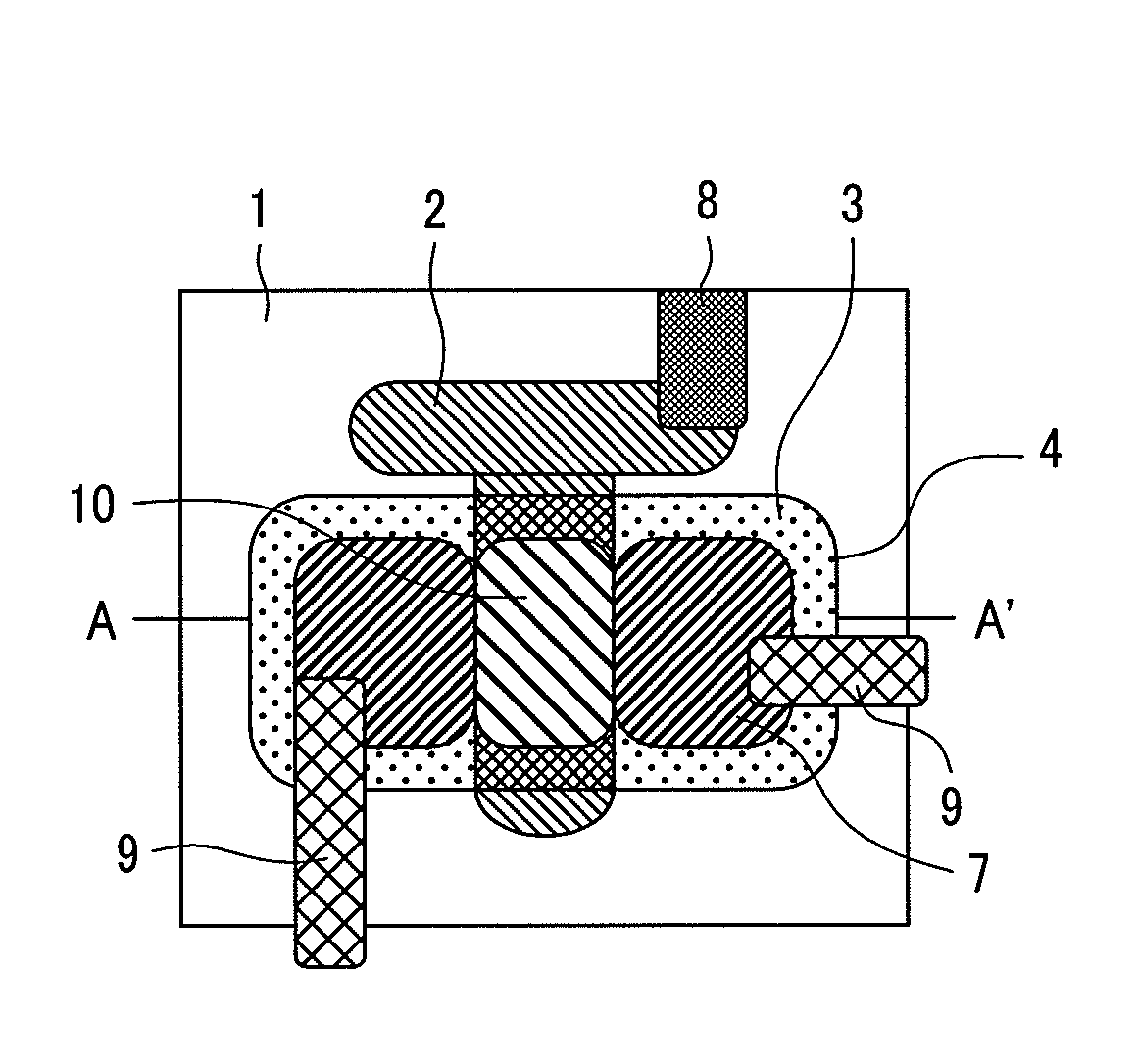
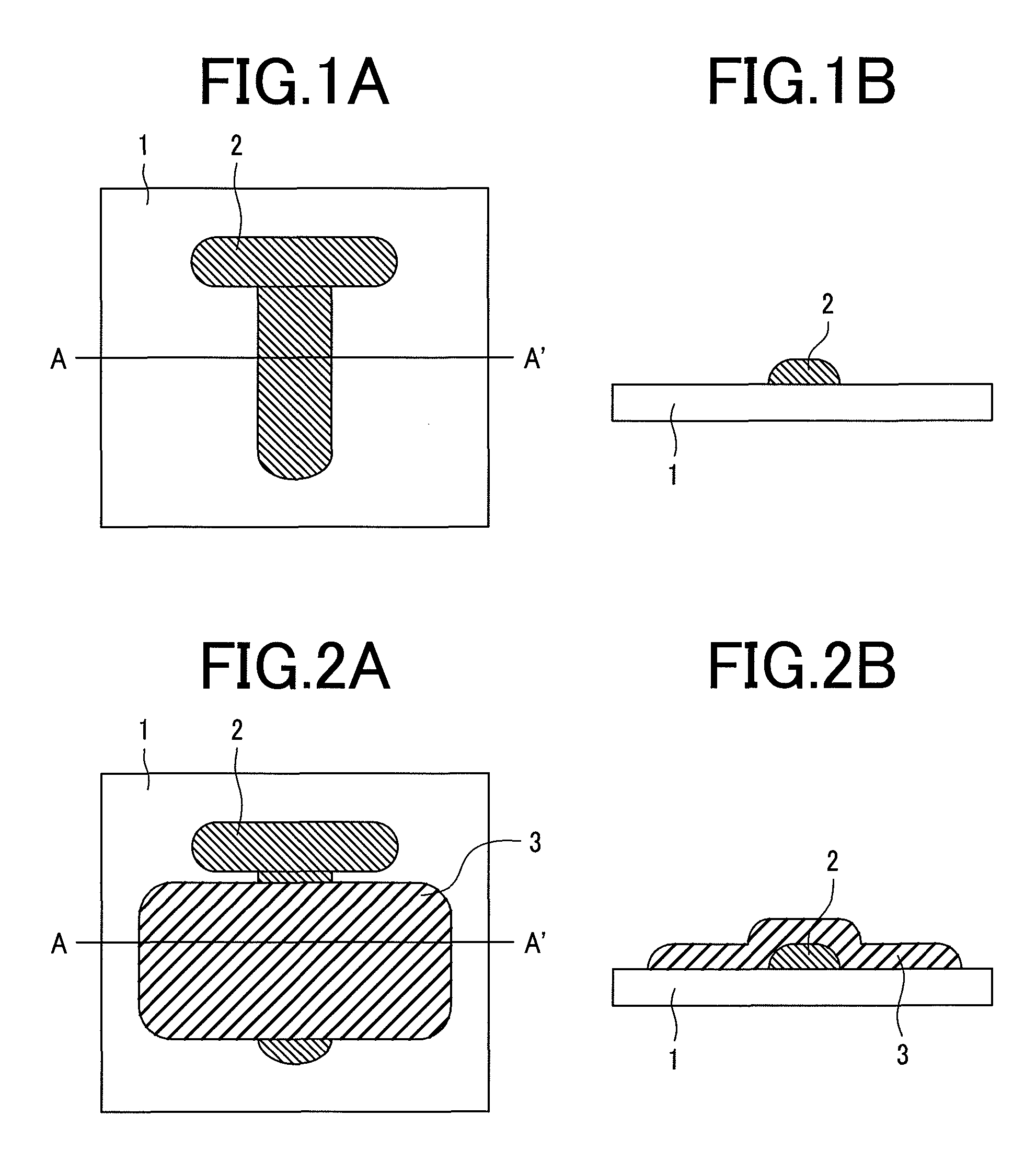
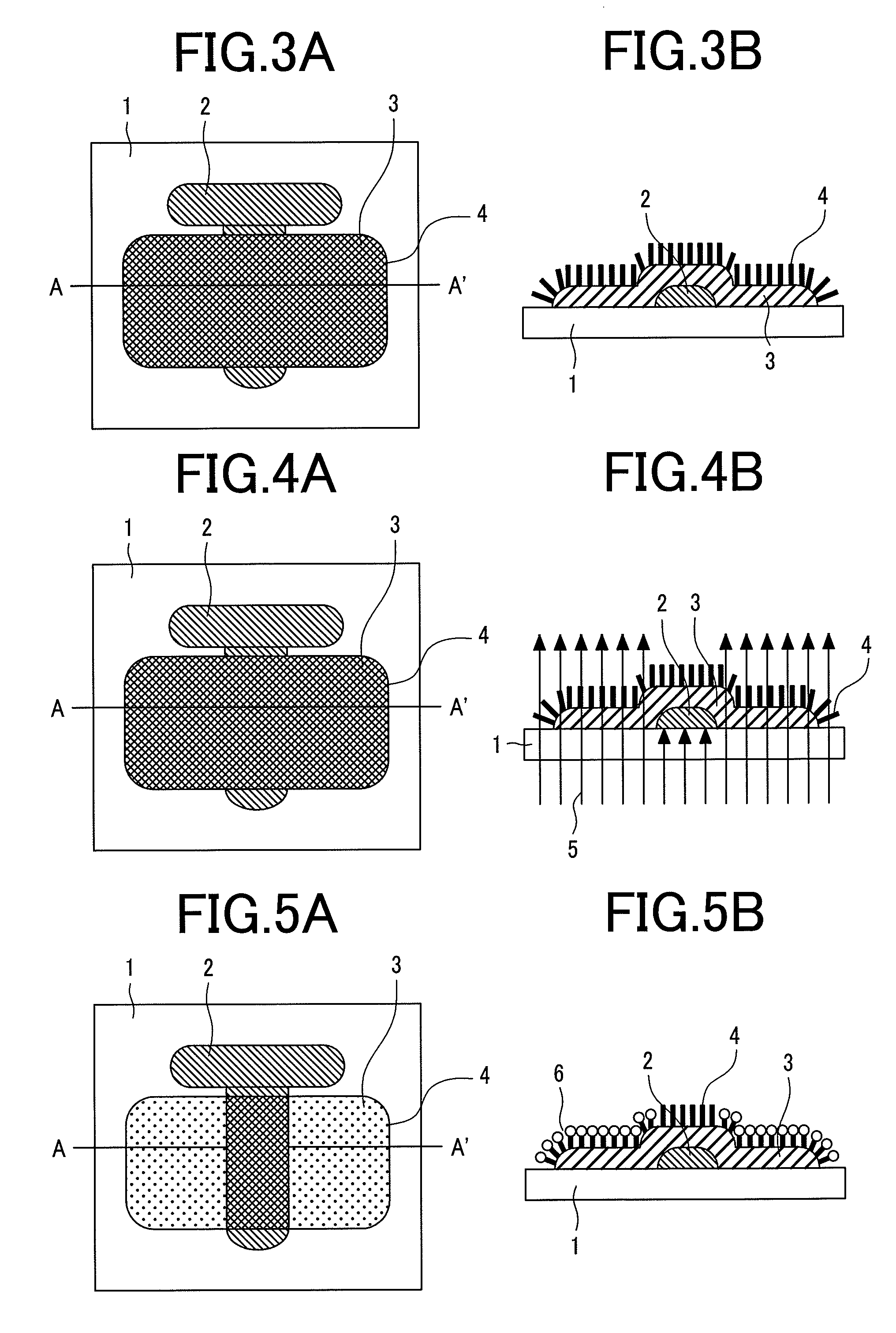
[0060]FIG. 1 to FIG. 8 are plan views and cross sectional views showing a device in the order of the manufacturing step to form source and drain electrodes by the exposure from the rear face of a substrate, according to a first embodiment. In each of the drawings, “A” is for the upper plan view and “B” is for a cross sectional view taken along line A-A′ in “A” of the drawings. In the upper plan views and the cross sectional views of the devices shown in the order of the manufacturing steps in the present specification, “A” is the upper plan view and “B” is the cross sectional view.

[0061]Polycarbonate as an organic compound was used for a transparent substrate 1, and a gate electrode shape of 20 μm line width was printed by using gold nano particles dispersed in a toluene solution as an ink by an ink jet printing method and heating the same at a temperature of 200° C. for 5 minutes to form a gold gate electrode 2 (upper plan view: FIG. 1A, cross sectional view: FIG. 1B). The height o...

second embodiment

[0067]This embodiment is an example of forming organic semiconductor transistors by the number of two (19, 20) by the same method as in the first embodiment. FIG. 9 and FIG. 10 show the upper plan view and the cross sectional view of this embodiment. While the method of forming each of the transistors is similar to that for the first embodiment described previously, a drain electrode 6 of a first transistor 19 and a gate electrode 2 of a second transistor 20 are connected by an interconnection 11 after forming each of the transistors in the configuration of the present embodiment. FIG. 9 shows an upper plan view and FIG. 10 shows a cross sectional view taken along cross section A-A′ in FIG. 9. The performance of both of the transistors was quite identical and transistors with less fluctuation of the performance could be prepared.

[0068]The first and the second embodiments show typical examples having particularly high performance in view of both the cost and the performance. Now, oth...

third embodiment

[0080]In this embodiment, an m×n active matrix type thin film transistor substrate comprising thin film transistors in m rows and n columns, and a manufacturing method thereof are to be described with reference to FIGS. 11 to 14. The active matrix type thin film transistor substrate is formed at intersections between m number of gate electrodes each constituting at least a portion of a lower electrode and n number of signal interconnections each constituting at least a portion of the upper electrode. Fundamental preparation procedures are similar to those for the first embodiment. At first, m number of gate interconnections / electrodes 2 in which n number of ring-shaped rectangles each having an opening and disposed in adjacent with each other are connected at least at one or more connection portions 17 (two positions in this embodiment) are disposed in close adjacent with each other by way of a gap 18 (upper plan view: FIG. 11A, cross sectional view: FIG. 11B). Particularly, by defi...


PUM

PropertyMeasurementUnit
temperatureaaaaaaaaaa
heat resistant temperatureaaaaaaaaaa
displacementaaaaaaaaaa

Abstract

An electrode substrate in which a lower electrode and an upper electrode are well positioned by way of an insulating film could not be formed by a printing method since positional displacement is caused. The cost was increased outstandingly when using photomasks for positioning. In the present invention, positional displacement does not occur even when using the printing method since the upper electrode and the lower electrode are positioned in self-alignment. Accordingly, a semiconductor device such as a flexible substrate using an organic semiconductor can be formed with low cost by using the printing method.

Description

CLAIM OF PRIORITY[0001]The present application claims priority from Japanese application JP 2006-149992, filed on May 30, 2006, the content of which is hereby incorporated by reference into this application.BACKGROUND OF THE INVENTION[0002]1. Field of the Invention[0003]The present invention relates to a method of manufacturing a semiconductor device having an organic thin film transistor.[0004]2. Description of the Related Art[0005]In recent years, various research and development have been conducted on display apparatus having TFT (Thin Film Transistor). Since TFTs are less power consuming and space saving, they have now been started for use as driving transistors for display devices in portable equipments such as mobile phone, notebook type personal computers, and PDAs. Such TFTs are manufactured mostly with inorganic semiconductor materials typically represented by crystalline silicon or amorphous silicon. This is because they can be manufactured by using existent manufacturing ...

Claims


Application Information

Patent Timeline
Patent Type & Authority Patents(United States)
IPC IPC(8): G03F7/26
CPCH01L51/0022H01L51/102H01L27/283H01L51/0545H10K19/10H10K71/611H10K10/466H10K10/82
Inventor ARAI, TADASHISHIBA, TAKEOANDO, MASAHIKOTORII, KAZUYOSHI
Owner HITACHI LTD
Why Eureka
Try Eureka