Multilayered wiring board, semiconductor device in which multilayered wiring board is used, and method for manufacturing the same

a multi-layer wiring and semiconductor technology, applied in the direction of printed circuit parts, printed circuit non-printed electric components association, printed circuit incorporation, etc., can solve the problems of board thickness, inability to meet the recent demand for higher density, and thick through-holes of boards, so as to reduce the risk of electrical peeling during heating, reduce the risk of electrical peeling, and reduce the effect of signal degradation during transmission

Active Publication Date: 2011-10-18
RENESAS ELECTRONICS CORP
View PDF19 Cites 21 Cited by
  • Summary
  • Abstract
  • Description
  • Claims
  • Application Information

AI Technical Summary

Benefits of technology

[0020]An object of the present invention is to provide a low-cost multilayered wiring board that has excellent high-speed, high-frequency characteristics, to provide a semiconductor device in which the multilayered wiring board is used, and to provide a method for manufacturing the same, by using an insulating resin composed of a photosensitive polyimide-based resin and PBO-based resin in which a diazonaphthoquinone-based (DNQ-based) material is used as a photosensitizer, and by avoiding the use of an adhesive layer composed of chromium, titanium, tungsten, molybdenum, tantalum, vanadium, nickel, or another material that reduces adhesion to the insulating resin and increases the resistance of the wiring layer covered by an insulation layer in which the wiring layout distance is increased.
[0028]In accordance with the present invention, conductor peeling during heating can be effectively prevented in a multilayered wiring board that uses a photosensitive polyimide material in which a diazonaphthoquinone-based (DNQ-based) material is used as a photosensitizer. Also, signal degradation during transmission can be minimized, and a multilayered wiring board having high-speed, high-frequency characteristics can be obtained without the use of a high-resistance adhesive layer as the wiring layer, which has a long wiring distance and is covered by the insulation layer.
[0029]In accordance with the method for manufacturing the wiring board of the present invention, the wiring board of the present invention can be efficiently fabricated, stable wire formation is made possible by using a support board in the steps, and future high-density and micro-wire formation can be achieved. Since the thickness of the wiring board can furthermore be minimized by removing the support board after wiring formation, inductance can be reduced and electrical loss can be suppressed.
[0030]In accordance with the method for manufacturing the semiconductor device according to the present invention, the semiconductor device according to the present invention can be effectively fabricated, and since the semiconductor elements are mounted while making use of the stable support board, connections can be stably made at a very narrow pitch of 50 μm or less. The thickness of the wiring board can furthermore be minimized by removing the support board after the semiconductor elements have been mounted, and the space between previously mounted semiconductor elements can be set to a very short distance by mounting another semiconductor element on the exposed surface. For this reason, a large number of micro-connections can be provided, and high-speed signal transmission and a wide bus width can be brought about between the semiconductor elements on the two surfaces.
[0031]Also, the support board can be reused and the costs reduced by peeling away the support board in the removal step.

Problems solved by technology

Built-up boards and other boards having through-holes have conventionally been commonly used as wiring boards, but boards having through-holes are thick and are furthermore not suited to high-speed signal transmission due to the presence of through-holes.
Tape boards and other thin boards, on the other hand, are also used, but such boards cannot meet the recent demand for higher density because the methods for manufacturing tape boards limit the wiring layers to one or two layers, and the pattern positioning accuracy is inferior to built-up boards due to considerable shrinkage of the tape material.
Photolithography must be used in order to form vias having a diameter of about 10 μm because of the difficultly of obtaining a required shape when laser-machining or dry-etching an insulating resin.
Nevertheless, the above-described methods for manufacturing the wiring boards and semiconductor devices in which a release layer is used have the following problems.
However, the diazonaphthoquinone-based (DNQ-based) materials have a problem in that these materials considerably reduce the adhesion of the boundary between the insulating resin and chromium, titanium, tungsten, molybdenum, tantalum, vanadium, nickel, and other materials used in the adhesive layer and that the conductive pattern peels away because decomposition products, reaction products, and other products of the material itself are produced during heating.

Method used


Image

  • Multilayered wiring board, semiconductor device in which multilayered wiring board is used, and method for manufacturing the same
  • Multilayered wiring board, semiconductor device in which multilayered wiring board is used, and method for manufacturing the same
  • Multilayered wiring board, semiconductor device in which multilayered wiring board is used, and method for manufacturing the same

Examples


first embodiment

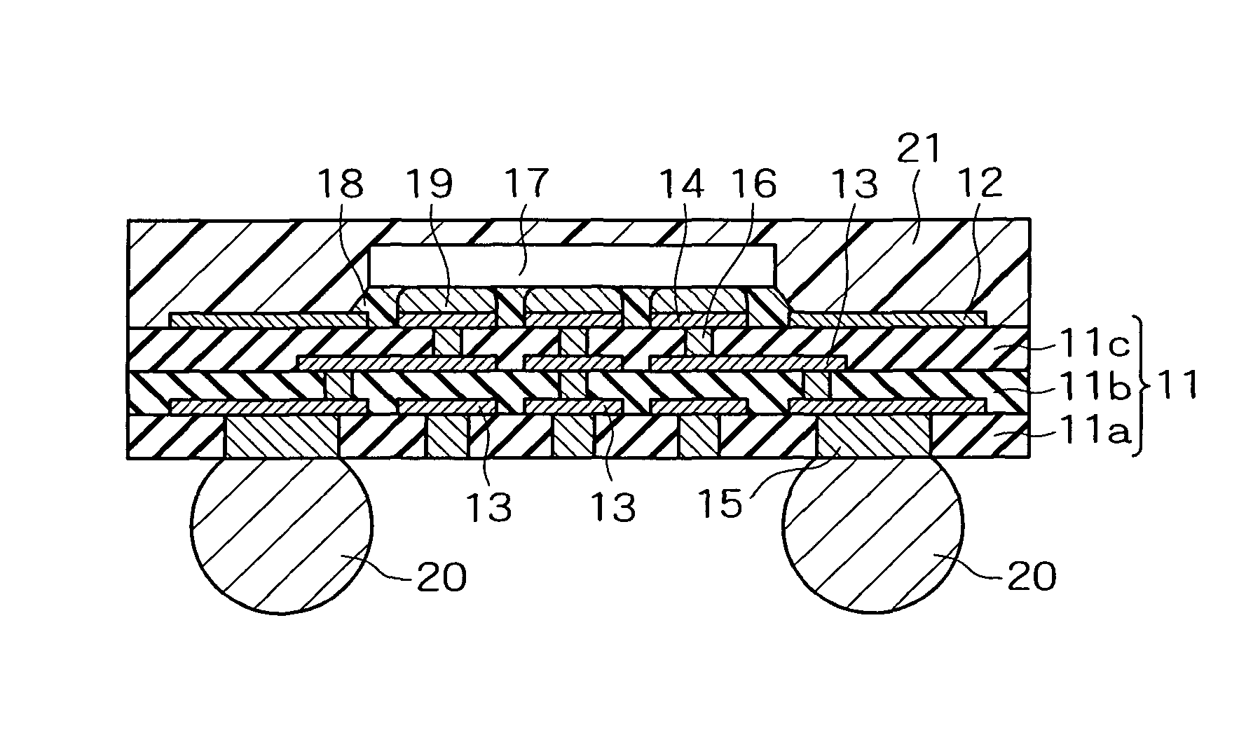
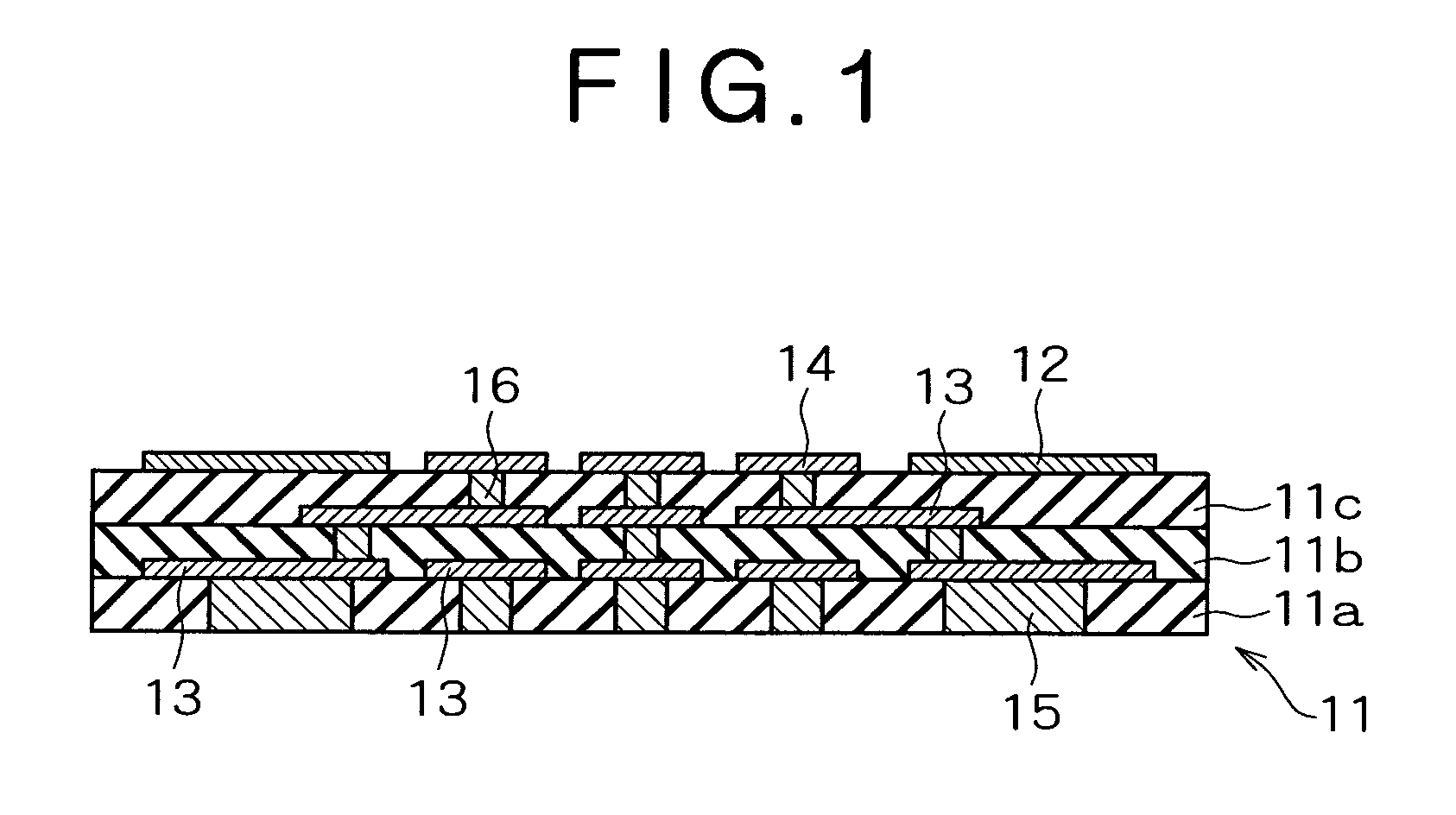
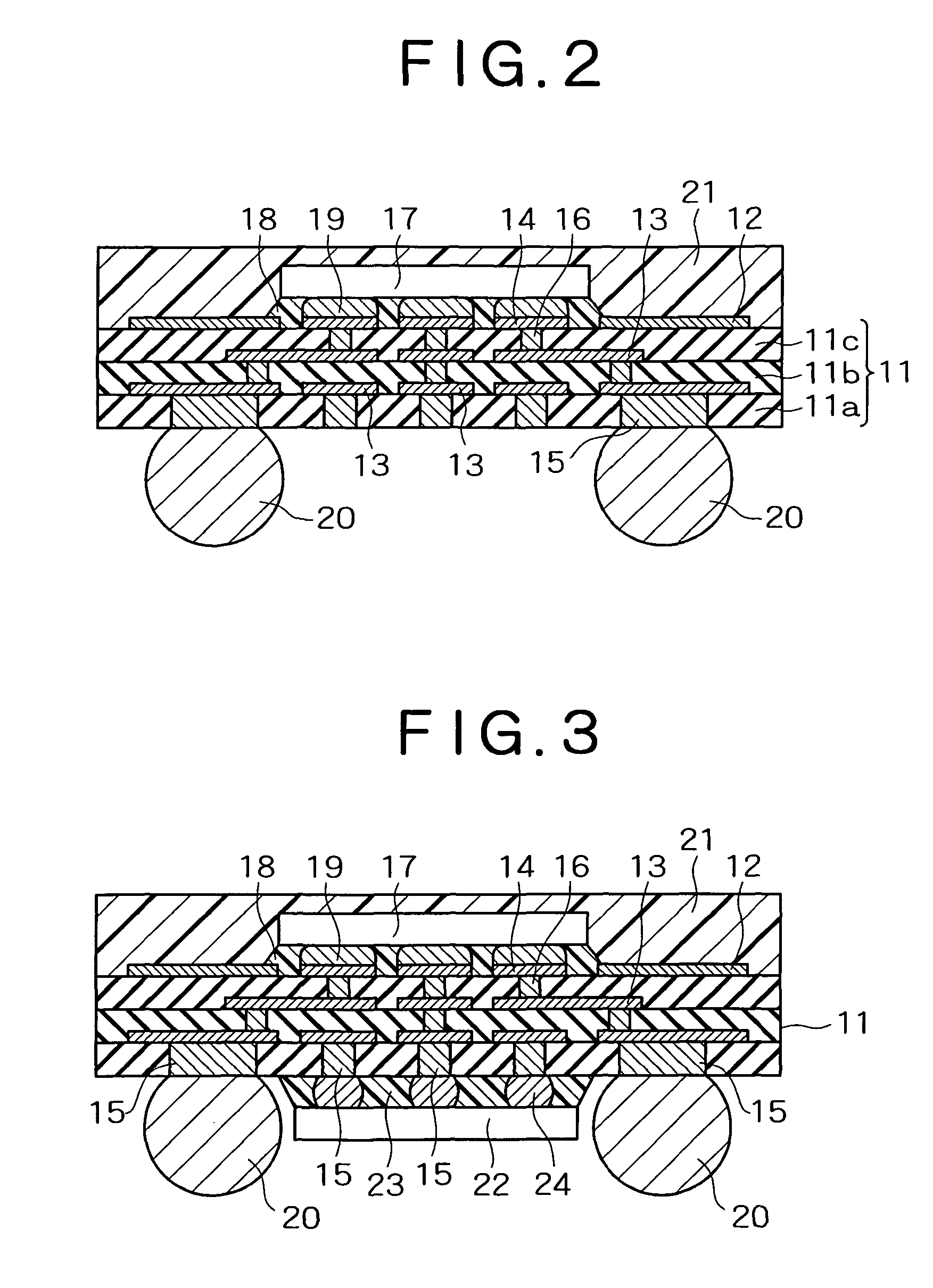
[0039]FIG. 1 is a local sectional view showing the multilayered wiring board according to the present invention. The multilayered wiring board shown in FIG. 1 has second electrodes 15 embedded in the bottommost insulation layer 11a. A second wiring layer 13 is formed on the insulation layer 11a and second electrodes 15, and an intermediate insulation layer 11b is formed so as to cover the insulation layer 11a and second electrodes 15, including the second wiring layer 13. Also, one or a plurality of pairs of the second wiring layer 13 and intermediate insulation layer 11b is disposed (a single pair in the diagram). The second wiring layer 13 is formed on the topmost (a single layer in the diagram) intermediate insulation layer 11b, and a topmost insulation layer 11c is formed so as to cover the intermediate insulation layer 11b, including the second wiring layer 13. First electrodes 14 and a first wiring layer 12 are formed on the topmost insulation layer 11c. Vias 16 provide electr...

second embodiment

[0052]FIG. 2 is a cross-sectional view showing the semiconductor device according to the present invention, and the wiring board shown FIG. 1 is used therein. In the FIG. 2, the second electrodes 15 disposed in the bottommost insulation layer 11a shown in FIG. 1 are shown as connected only to the solder balls 20. Accordingly, in FIG. 2, the same reference numerals are used for the same constituent elements as FIG. 1, and a detailed description of the multilayered wiring board shown in FIG. 1 is omitted.

[0053]The semiconductor device shown in FIG. 2 has a semiconductor element 17 mounted on the first electrodes 14 of the topmost insulation layer 11c of the multilayered wiring board shown in FIG. 1. The diagram shows only a single semiconductor element 17, but a plurality of semiconductor elements may be mounted, and capacitors, resistors, and other components may also be mounted.

[0054]The semiconductor element 17 is configured so that electrodes (not shown) on the surface of the semi...

fifth embodiment

[0081]FIG. 6A corresponds to the step shown in FIG. 5C in the method for manufacturing a semiconductor device of the fifth embodiment, and shows the step prior to removing the support board 25. The steps preceding the step shown in FIG. 5C are the same as the steps shown in FIGS. 4 and 5. Washing and heating treatments are suitably carried out between each step.

[0082]First, the second electrodes 15, insulation layer 11, first wiring layer 12, second wiring layer 13, and first electrodes 14 are formed on the support board 25, as shown in FIG. 6A. In the present invention, an insulation layer 11a is provided by forming a photosensitive polyimide resin to a thickness of 7 μm on a support board 25 in which a release layer (not shown) and an electroconductive seed metal layer (not shown) are sequentially disposed on a silicon wafer that has a thickness of 0.725 mm and a diameter of 8 inches (200 mm) and that is provided with a thermal oxidation layer. The second electrodes 15 are formed ...


PUM

PropertyMeasurementUnit
diameteraaaaaaaaaa
thicknessaaaaaaaaaa
peel strengthaaaaaaaaaa

Abstract

A multilayered wiring board has electrodes disposed on a first surface and a second surface, alternately layered insulation layers and wiring layers, and vias that are disposed in the insulation layer and electrically connect the wiring layers. The second electrode disposed on the second surface is embedded in the insulation layer exposed on said second surface, and the second wiring layer covered by the insulation layer exposed on said second surface does not have a layer for improving adhesion to the insulation layer.

Description

BACKGROUND OF THE INVENTION[0001]1. Field of the Invention[0002]The present invention relates to a wiring board on which a semiconductor element is mounted, a semiconductor device in which a semiconductor element is mounted on the wiring board, and a method for manufacturing the same, and more particularly relates to a thin multilayered wiring board having excellent high-speed transmission characteristics and to a semiconductor device that uses the wiring board.[0003]2. Description of the Related Art[0004]Electronic devices are rapidly becoming smaller, thinner, and increasingly dense, as recently seen in mobile equipment, and greater thinness, lighter weight, higher density, and other characteristics are needed in wiring boards used in device and semiconductor element mounting due to the increase in the number of terminals that is associated with higher speeds and functionality of semiconductor elements.[0005]Built-up boards and other boards having through-holes have conventionally...

Claims


Application Information

Patent Timeline
Patent Type & Authority Patents(United States)
IPC IPC(8): H05K1/16
CPCH01L21/6835H01L23/49822H05K3/4007H05K3/4644H01L23/49816H01L2924/181H01L2221/68345H01L2924/01046H01L2924/01057H01L2924/01078H01L2924/01079H01L2924/09701H01L2924/15311H01L2924/1532H01L2924/19041H01L2924/3011H05K3/0023H05K3/205H05K2201/0367H05K2203/0733H01L2924/01322Y10T29/49128Y10T29/4913H01L2224/73204H01L2224/32225H01L2224/16225H01L2924/00012H01L2924/00H01L24/16H01L2221/68381H01L24/32H01L2224/81005
Inventor KIKUCHI, KATSUMIYAMAMICHI, SHINTAROKURITA, YOICHIROSOEJIMA, KOJI
Owner RENESAS ELECTRONICS CORP
Why Eureka
Try Eureka