Device for cleaning CVD device and method of cleaning CVD device

a technology of cvd device and cleaning method, which is applied in the direction of cleaning hollow articles, chemistry apparatus and processes, coatings, etc., can solve the problems of deterioration of yield or the like, contamination in the film forming process, and yield or the like might also be deteriorated, so as to achieve high gas utilization efficiency and enhance productivity.

Active Publication Date: 2011-10-25
CANON ANELVA CORP +4
View PDF22 Cites 4 Cited by
  • Summary
  • Abstract
  • Description
  • Claims
  • Application Information

AI Technical Summary

Benefits of technology

[0028]In consideration of such circumstances, it is an object of the present invention to provide an apparatus for cleaning a CVD apparatus which can efficiently remove a by-product such as SiO2 or Si3N4 stuck and deposited onto the surface of an internal wall, an electrode or the like in a reaction chamber in a film forming process, and furthermore, can execute cleaning in which the amount of a cleaning gas to be discharged is very small, an influence on an environment such as global warming is small, a gas utilization efficiency is high and a productivity can also be enhanced, and a method for cleaning a CVD apparatus using the same cleaning apparatus.

Problems solved by technology

The by-product is peeled by a dead weight, a stress or the like when it grows to have a constant thickness, and particulates are mixed as foreign matters into a semiconductor product, thereby causing a contamination in the film forming process.
Thus, a thin film of high quality cannot be manufactured so that the disconnection or short circuit of a semiconductor circuit might be caused, and furthermore, a yield or the like might also be deteriorated.
When the CVD apparatus is used repetitively, consequently, particulates are mixed into a semiconductor product, resulting in a contamination as described above.
Therefore, a thin film of high quality cannot be manufactured so that the disconnection or short circuit of a semiconductor circuit is caused, and furthermore, a yield or the like is also deteriorated.
Consequently, there is a possibility that an environment might be adversely influenced.
Moreover, there is a problem in that a gas discharging process is hard to perform after the cleaning and the cost of the process is high.
If the time required for the cleaning is thus prolonged, moreover, a throughput is reduced so that a productivity is deteriorated.

Method used


Image

  • Device for cleaning CVD device and method of cleaning CVD device
  • Device for cleaning CVD device and method of cleaning CVD device
  • Device for cleaning CVD device and method of cleaning CVD device

Examples


Embodiment Construction

[0126]Embodiments (examples) of the present invention will be described below in more detail with reference to the drawings.

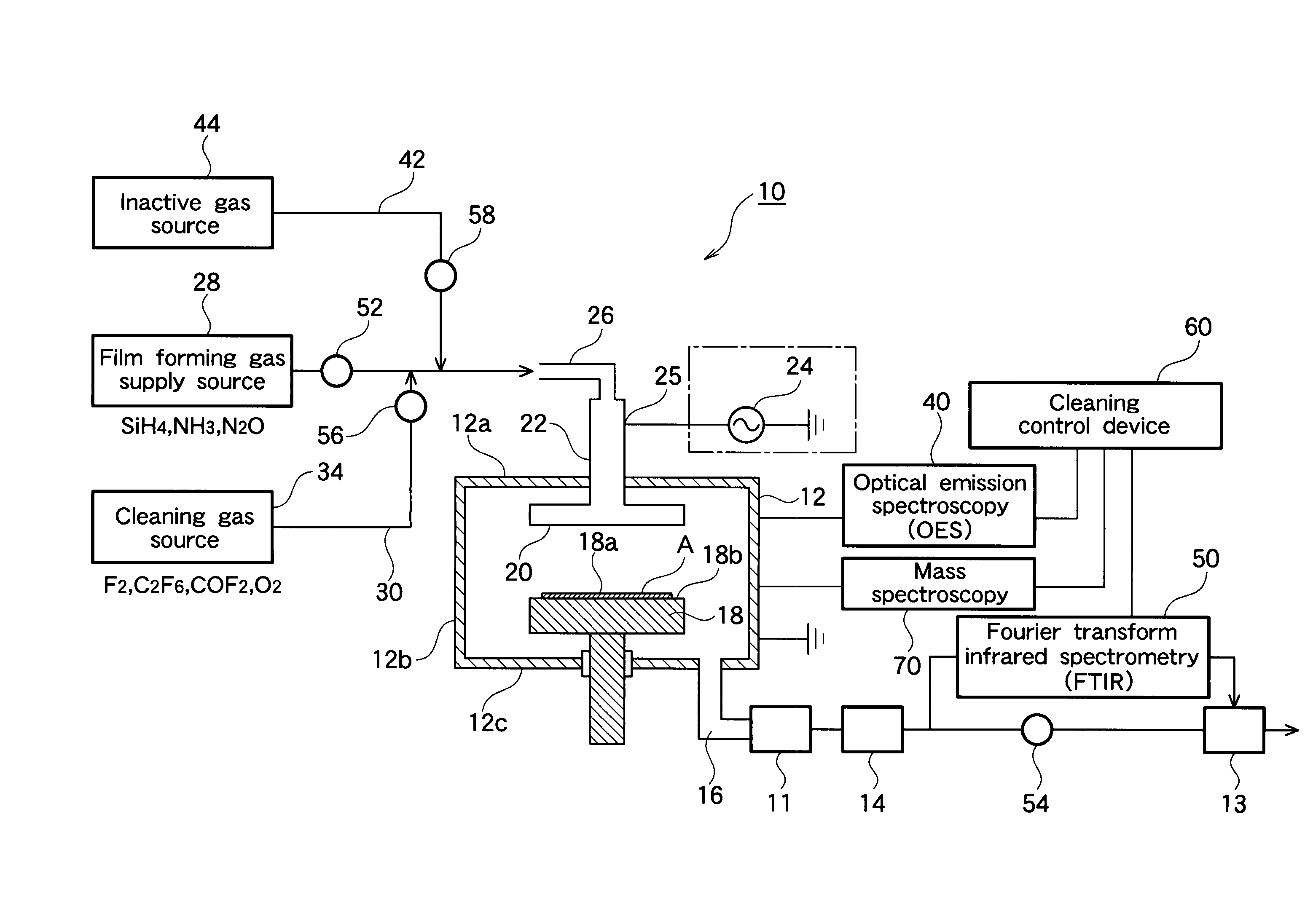
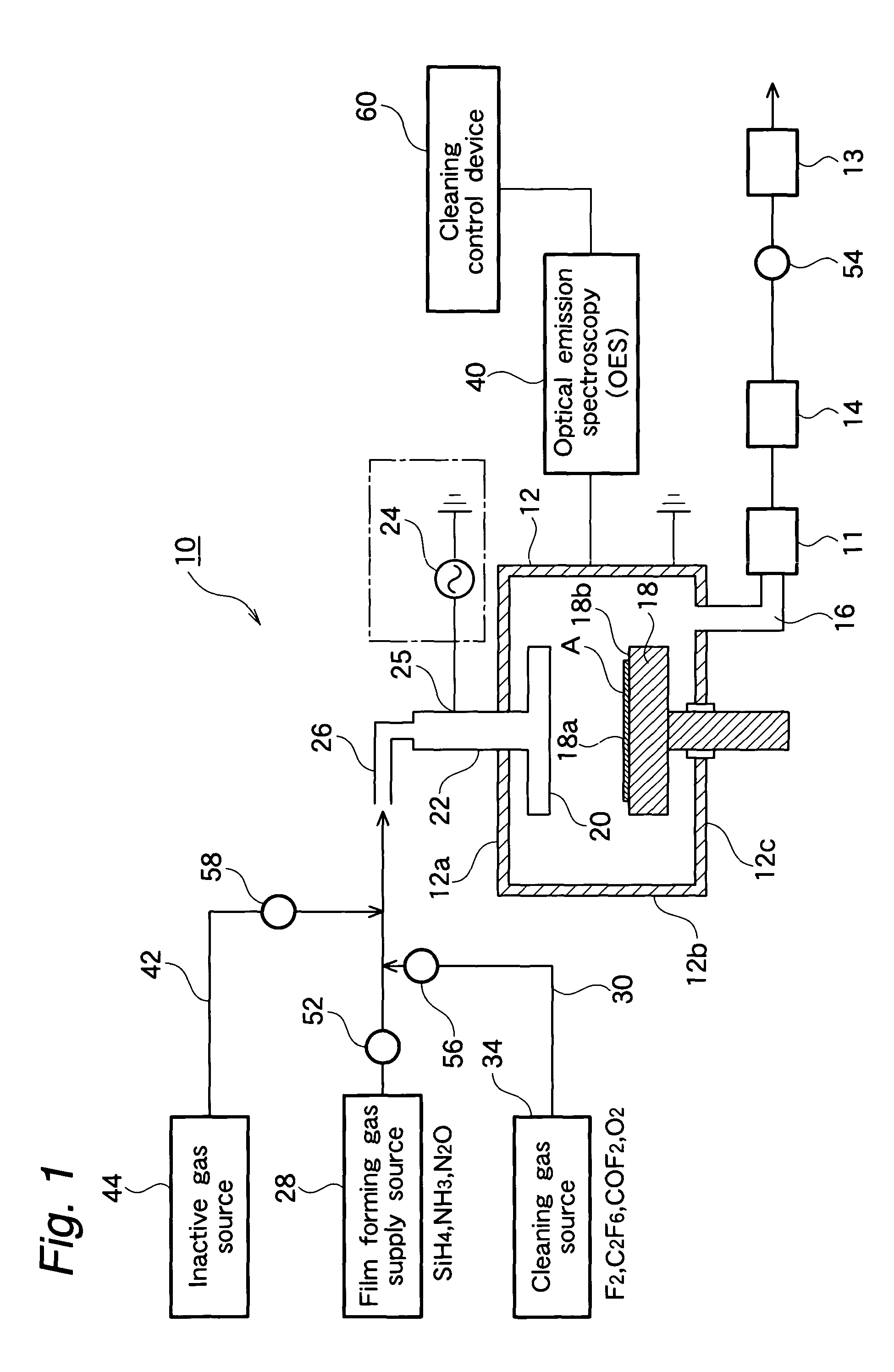
[0127]FIG. 1 is a schematic view showing an example in which an apparatus for cleaning a CVD apparatus according to the present invention is applied to the CVD apparatus.

[0128]As shown in FIG. 1, a plasma CVD apparatus 10 to be used in a plasma CVD method comprises a reaction chamber 12 maintained in a pressure reducing state (a vacuum state), and is maintained in a constant vacuum state (a pressure reducing state) by discharging an internal gas to an outside by means of a mechanical booster pump 11, a dry pump 14 and a harm removing device 13 for causing an exhaust gas to be non-toxic through an exhaust path 16 formed on a bottom wall 12c of the reaction chamber 12.

[0129]Moreover, a lower electrode 18 constituting a stage (a counter electrode stage) for mounting a base material A to accumulate (containing deposition) a thin silicon film on the surface of a sil...


PUM

PropertyMeasurementUnit
timeaaaaaaaaaa
timeaaaaaaaaaa
pressureaaaaaaaaaa

Abstract

An apparatus for cleaning a CVD apparatus that can efficiently remove a by-product such as SiO2 or Si3N4 stuck and deposited onto the surface of an internal wall, an electrode, or the like in a reaction chamber in a film forming process, and a method for cleaning a CVD apparatus. A control monitors luminous intensity data of an F radical in a reaction chamber by optical emission spectroscopy and compares the data with calibrated prestored luminous intensity data, and ends cleaning after a predetermined time passes from reaching a luminous intensity saturation point. Furthermore, concentration data of SiF4 in a gas discharged from the reaction chamber are monitored by a Fourier transform infrared spectrometry and compared with prestored concentration data of SiF4 to decide that the predetermined time has passed when a predetermined cleaning end point concentration is reached, thereby ending the cleaning.

Description

TECHNICAL FIELD[0001]The present invention relates to a chemical vapor deposition (CVD) apparatus for forming a uniform thin film of high quality, for example, silicon oxide (SiO2) or silicon nitride (Si3N4 or the like) on the surface of a base material for a semiconductor such as a silicon wafer.[0002]In more detail, the present invention relates to an apparatus for cleaning a CVD apparatus which can execute cleaning and removing a by-product stuck to the internal wall of a reaction chamber or the like after a thin film forming process, and a method for cleaning the CVD apparatus using the same.BACKGROUND ART[0003]Conventionally, a thin film such as silicon oxide (SiO2) or silicon nitride (Si3N4 or the like) has been used widely for a semiconductor device such as a thin film transistor, a photoelectric converting device or the like. The following three kinds of methods are mainly used as a method of forming the thin film such as the silicon oxide or the silicon nitride.[0004](1) Ph...

Claims


Application Information

Patent Timeline
Patent Type & Authority Patents(United States)
IPC IPC(8): B08B9/00C23C16/44C23C16/52H01L21/31
CPCC23C16/4405C23C16/52
Inventor SAKAI, KATSUOABE, KAORUOKURA, SEIJISAKAMURA, MASAJIMURATA, HITOSHIKAMEDA, KENJIWANI, ETSUOSEKIYA, AKIRA
Owner CANON ANELVA CORP
Why Eureka
Try Eureka