Adsorption based material removal process

a technology of adsorption and material, applied in the direction of decorative arts, decorative surface effects, electric devices, etc., can solve the problems of limited halogen-silicon chemistry, limited methods for controlling the removal of one or several atomic layers, and inapplicability to other materials of the ic device, such as silicon dioxid

Inactive Publication Date: 2011-10-25
NOVELLUS SYSTEMS
View PDF80 Cites 388 Cited by
  • Summary
  • Abstract
  • Description
  • Claims
  • Application Information

AI Technical Summary

Problems solved by technology

While atomic layer deposition (ALD) and atomic-scale epitaxial growth techniques have been developed, the methods for controlled removal of one or several atomic layers are still limited.
This technique, although valuable for its purpose of semiconductor etching, is limited to the halogen-silicon chemistry and is not widely applicable.
For instance, it cannot be applied to other materials of the IC device, such as silicon dioxide.
Furthermore, sputtering during the desorption step is often damaging to the wafer components since it involves bombardment of the wafer surface with high-energy species.
As in the case of silicon ALET, the described chemistry is not widely applicable.
The method also necessarily involves irradiation with high-energy ions, which may be damaging to the wafer.
None of the described above methods is applicable to etching of SiO2 on an atomic scale.
It also is inadvertently formed on the layers of silicon when the partially fabricated wafer is exposed to air.
Native oxide film together with oxide residue produced during etching and / or ashing frequently presents a problem for further processing steps.
This requirement limits the number of practically feasible pre-clean methods to dry etching processes, which will be discussed further.
It should be understood, that none of these methods can accomplish a well controlled removal of one or several atomic layers of silicon dioxide.
All of the methods described below remove bulk amounts of silicon dioxide and are poorly controlled at an atomic level.
This method, however, is rarely used due to corrosive properties of HF / H2O mixtures, which may damage the process chamber.
Ammonium fluoride and ammonium bifluoride cannot be easily introduced into the dry-etch chamber, due to their relatively low vapor pressure, and are most often formed from gaseous precursors within the chamber.
These CVD-type processes are not well suited to accurately control the thickness of a layer to be removed and cannot be applied for removal of defined amounts of material on an atomic scale.
Although in some cases the amount of deposited etchant can be controlled by the use of microbalance, it is not possible to achieve accurate atomic layer control over material removal by these types of methods.
Thus an uncontrolled amount of etchant is brought into contact with the on the wafer surface.
Although this proposed method may provide some fine control over the etching process, it is laborious and imprecise due to difficulties in QCM calibration.
The CVD-type etchant deposition processes are poorly controlled at an atomic level.
These methods are also not well suited for etching relatively small amounts of material, particularly from the high aspect ratio features of the substrate.
While these methods sometimes work adequately in the substrates with low aspect ratio features, they do not provide highly conformal and uniform etchant film coverage needed for removal of material from high aspect ratio recesses.
The amount of deposited etchant, and, consequently, the amount of etched material is limited by the amount of adsorbed first reactant.

Method used


Image

  • Adsorption based material removal process
  • Adsorption based material removal process
  • Adsorption based material removal process

Examples


Embodiment Construction

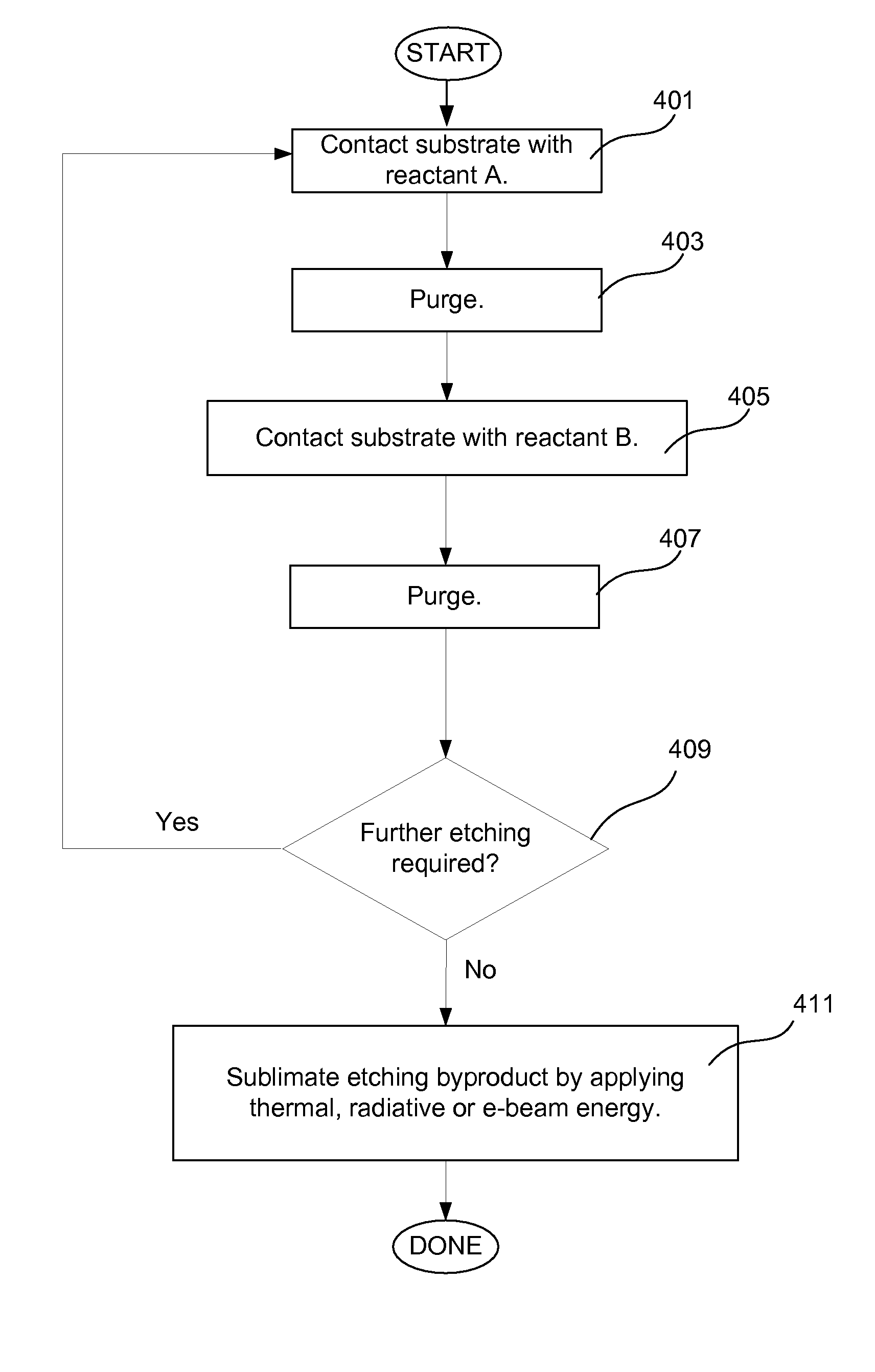
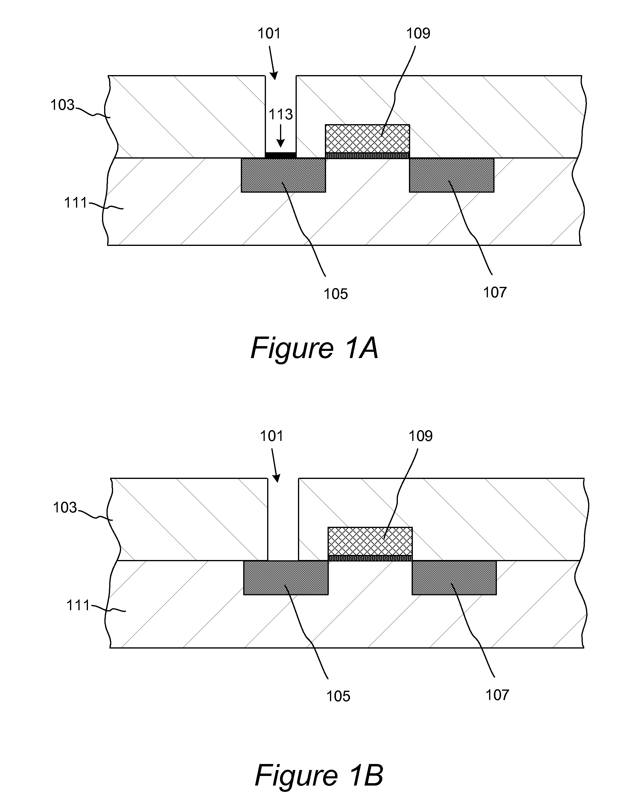
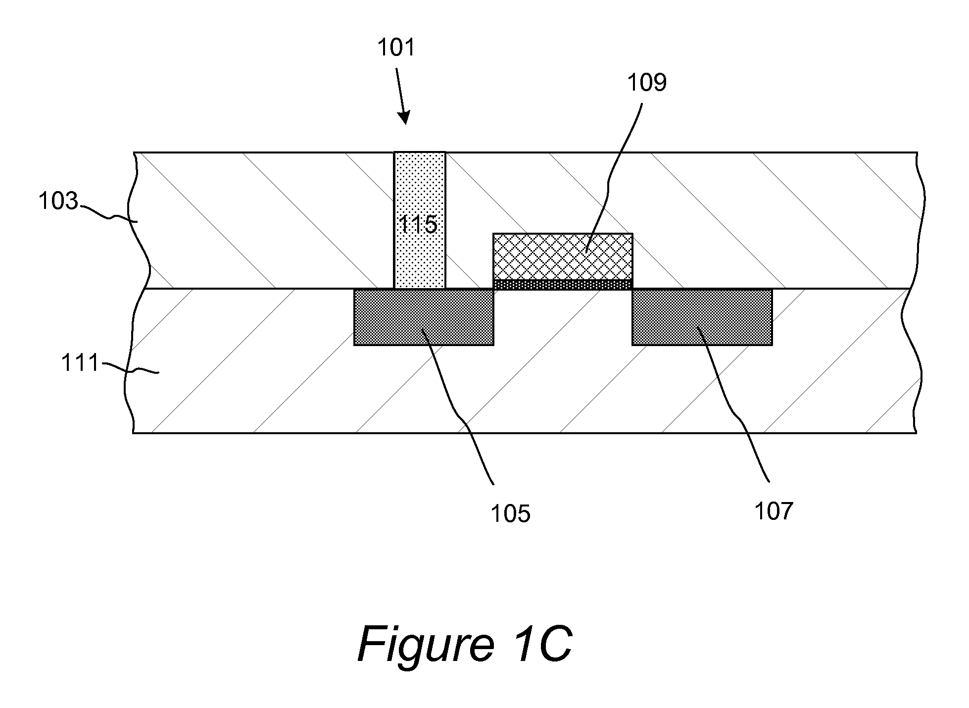
[0041]Aspects of the present invention are directed to atomic layer removal (ALR™) of materials from substrates, such as partially fabricated integrated circuits. While the methods of present invention find particular use in the processing of semiconductor substrates, they can also be employed in other applications, such as removal of oxide material from other workpieces such as those employed in flat panel display manufacturing. ALR™ methods achieve accurate and conformal removal of material on small scales not feasible with prior techniques, e.g. on scales of about 160 Å or smaller. In fact, they can be employed when removal of layers of only several angstroms or tens of angstroms is desired. Atomic layer removal methods allow control of the depth of etching by repeating deposition of etchant cycles, where each cycle may remove as little as only a monolayer or submonolayer of material. These methods can be performed in a CVD-type apparatus, and can be easily integrated with existi...


PUM

PropertyMeasurementUnit
depthaaaaaaaaaa
depthaaaaaaaaaa
depthaaaaaaaaaa

Abstract

Methods for accurate and conformal removal of atomic layers of materials make use of the self-limiting nature of adsorption of at least one reactant on the substrate surface. In certain embodiments, a first reactant is introduced to the substrate in step (a) and is adsorbed on the substrate surface until the surface is partially or fully saturated. A second reactant is then added in step (b), reacting with the adsorbed layer of the first reactant to form an etchant. The amount of an etchant, and, consequently, the amount of etched material is limited by the amount of adsorbed first reactant. By repeating steps (a) and (b), controlled atomic-scale etching of material is achieved. These methods may be used in interconnect pre-clean applications, gate dielectric processing, manufacturing of memory devices, or any other applications where removal of one or multiple atomic layers of material is desired.

Description

CROSS REFERENCE TO RELATED APPLICATION[0001]This application is a continuation of application Ser. No. 11 / 479,812 filed Jun. 30, 2006 now U.S. Pat. No. 7,416,989 and titled ADSORPTION BASED MATERIAL REMOVAL PROCESS which is incorporated by reference herein in its entirety and for all purposes.FIELD OF THE INVENTION[0002]The present invention pertains to methods of removing layers of material on a substrate. The methods are particularly useful for accurate and conformal removal of atomic layers of oxide material such as silicon dioxide on a partially fabricated integrated circuit. As examples, the methods can be applied for pre-clean operations, for fabrication of gate dielectric in transistors, and for fabrication of memory and logic devices.BACKGROUND OF THE INVENTION[0003]Fabrication of integrated circuit (IC) devices at a modern level of miniaturization demands techniques that can operate at an atomic scale. Certain components of IC devices now have dimensions of tens or hundreds...

Claims


Application Information

Patent Timeline
Patent Type & Authority Patents(United States)
IPC IPC(8): H01L21/302
CPCH01L21/02063H01L21/31116H01L21/6708
Inventor LIU, XINYECOLLINS, JOSHUAASHTIANI, KAIHAN A.
Owner NOVELLUS SYSTEMS
Why Eureka
Try Eureka