IP cores in reconfigurable three dimensional integrated circuits

a three-dimensional integrated circuit and core technology, applied in the field of ip cores, can solve the problems of limiting the responsiveness of specific types of applications, all four have limits, and the approach is limited to optimizing arithmetic-intensive applications, so as to increase flexibility for customers, save substantial time and resources in designing, and reduce the time to market of specific applications

Inactive Publication Date: 2011-10-25
SOLOMON RES
View PDF3 Cites 36 Cited by
  • Summary
  • Abstract
  • Description
  • Claims
  • Application Information

AI Technical Summary

Benefits of technology

[0041]The present invention uses IP cores for 3D ICs that provide numerous advantages. First, customers save substantial time and resources in designing and testing the chip by programming, and reprogramming, it after production. Second, customer time to market of specific applications is vastly reduced by production of a generic hardware architecture and later implementation of IP cores. Application functions can thus be designed after chip production. This increases flexibility for customers.
[0042]The IP designs are reusable, particularly because they combine 3D IP core elements in unique configurations. The use and recombination of 3D IP core elements allow the development of complex applications for indeterministic continuous reprogrammability using the iSoC.
[0080]WSPS, wafer level processed stack packages

Problems solved by technology

The challenge of modern computing is to build economically efficient chips that incorporate more transistors to meet the goal of achieving Moore's law of doubling performance every two years.
The limits of semiconductor technology are affecting this ability to grow in the next few years, as transistors become smaller and chips become bigger and hotter.
Like some supercomputing applications, this approach is limited to optimizing arithmetic-intensive applications such as modeling.
However, all four also have limits.
The multi-core architecture has a problem of synchronization of the parallel micro-processors that conform to a single clocking model.
This problem limits their responsiveness to specific types of applications, particularly those that require rapid environmental change.
Further, the multi-core architecture requires “thread-aware” software to exploit its parallelism, which is cumbersome and produces quality of service (QoS) problems and inefficiencies.
By emphasizing its compiler, the TRIPS architecture has the problem of optimizing the coordination of scheduling.
This bottleneck prevents peak performance over a prolonged period.
The Cell architecture requires constant optimization of its memory management system, which leads to QoS problems.
Though targeted at the communications industry, particularly wireless communications, the chip has limits of flexibility that it was designed to overcome, primarily in its deterministic IP core application software.
While these hybrids are architecturally interesting, they possess the limits of each type of design paradigm, with restricted microprocessor performance and restricted deterministic IP core application software.
Though they have higher performance than a typical single core microprocessor, they are less flexible than a pure FPGA model.
However, this 3D chip approach of stacking existing 2D planar IC layers is generally limited to three or four layers.
However, these chips have only adjacent layer connectivity.
While planar design chips are easier to make, they are not generally high performance.
Prior systems demonstrate performance limits, programmability limits, multi-functionality limits and logic and memory bottlenecks.
There are typically trade-offs of performance and power.
Problems that the System Solves
One of the chief problems is to identify ways to limit latency.
Latency represents a bottleneck in an integrated circuit when the wait to complete a task slows down the efficiency of the system.
Examples of causes of latency include interconnect routing architectures, memory configuration and interface design.

Method used


Image

  • IP cores in reconfigurable three dimensional integrated circuits
  • IP cores in reconfigurable three dimensional integrated circuits
  • IP cores in reconfigurable three dimensional integrated circuits

Examples


Embodiment Construction

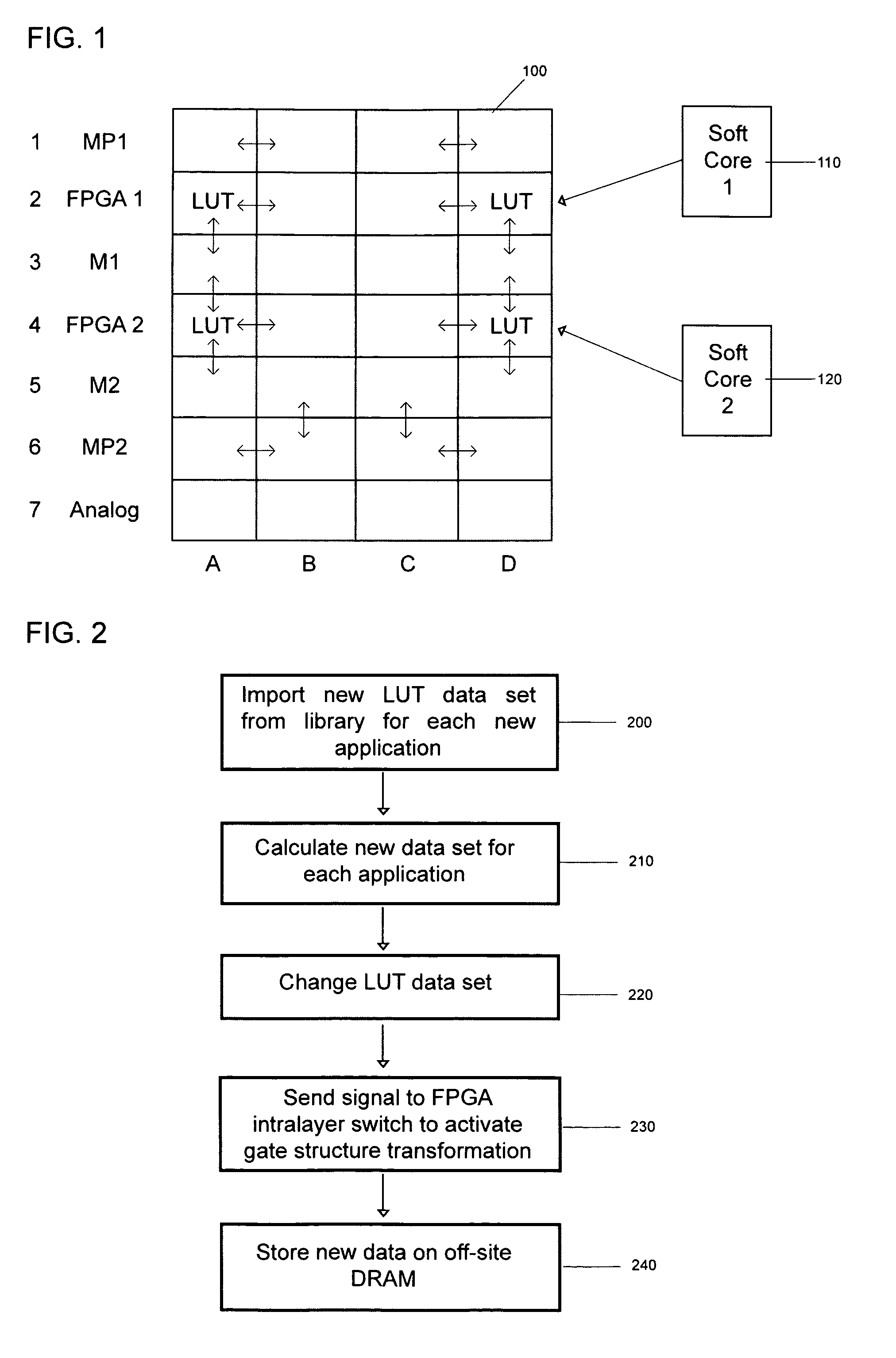
[0114]FIG. 1 shows the side view of a multilayer hybrid IC. Layers 1 and 6 consist of microprocessors, layers 2 and 4 consist of FPGAs, layers 3 and 5 consist of memory components and layer 7 consists of analog components. LUTs are in the outside edges of the FPGA layers. The arrows indicate the interactions between tiles in the IC. Soft core 1 (110) interacts with a LUT on FPGA 1, while soft core 2 (120) interacts with a LUT on FPGA 2. The soft cores update the program code on the FPGAs.

[0115]FIG. 2 is a flow chart of a process for the organization of netlists to store new data in a LUT. Once LUT data sets are imported from a library for each new application (200), a new data set are calculated for each application (210). The LUT data set is then changed (220) and a signal is sent to the FPGA intra-layer switch to activate the gate structure transformation (230) to reorganize the FPGA gate arrays. New data is then stored on off-site DRAM (240) components.

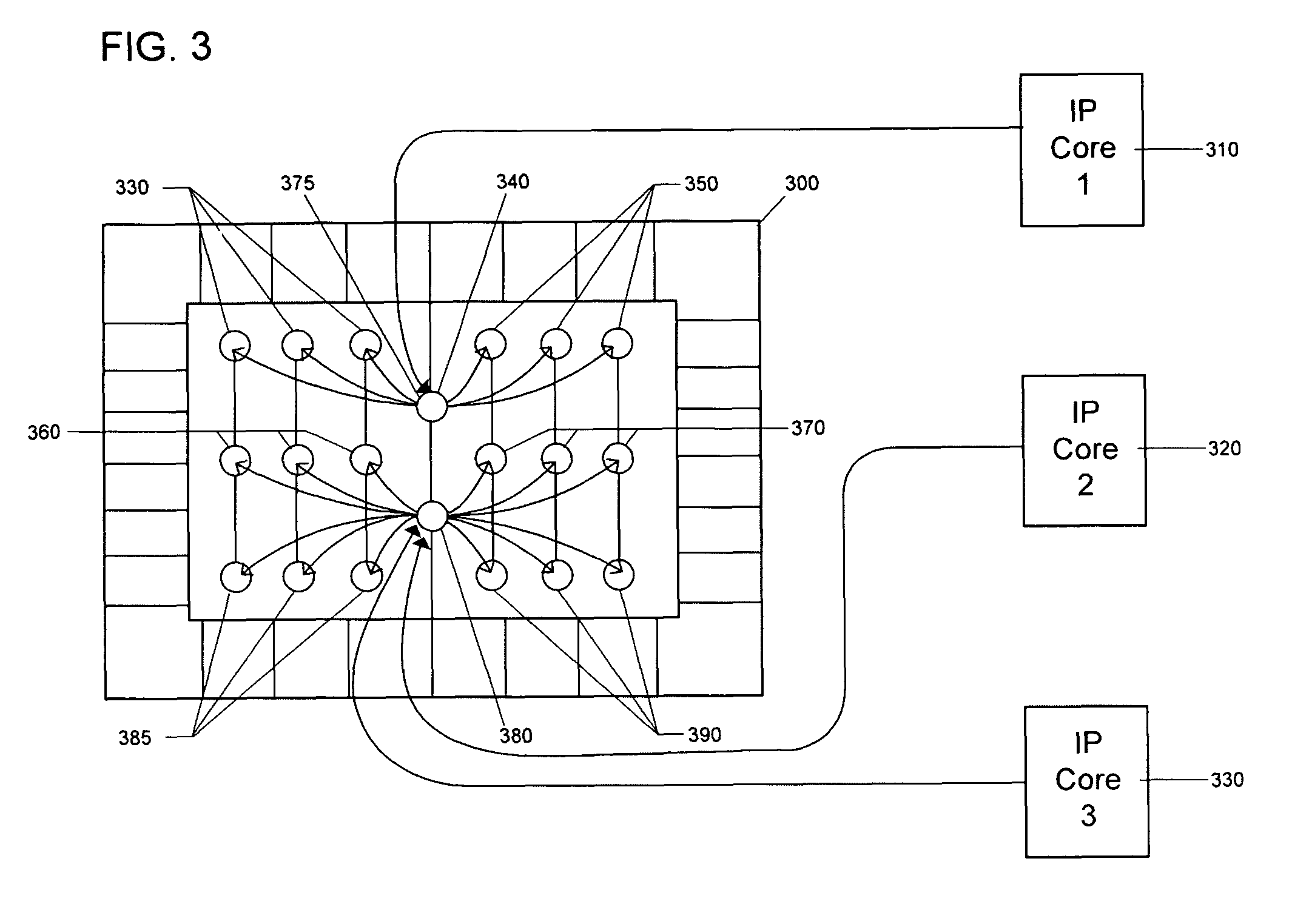
[0116]FIG. 3 shows the load...


PUM


Abstract

The invention describes IP cores applied to 3D FPGAs, CPLDs and reprogrammable SoCs. IP cores are (a) used for continuously evolvable hardware using 3D logic circuits, (b) applied with optimization metaheuristic algorithms, (c) applied by matching combinatorial logic of netlists generated by Boolean algebra to combinatorial geometry of CPLD architecture by reaggregating IP core elements and (d) used to effect continuous recalibration of IP cores with evolvable hardware in indeterministic environments for co-evolutionary reprogrammability.

Description

CROSS-REFERENCES TO RELATED APPLICATIONS[0001]The present application claims the benefit of priority under 35 U.S.C. §119 from U.S. Provisional Patent Application Ser. No. 60 / 993,580, filed on Sep. 12, 2007, the disclosure of which is hereby incorporated by reference in their entirety for all purposes.FIELD OF THE INVENTION[0002]The invention involves IP cores for reconfigurable system on chip (SoC) and network on chip (NoC) semiconductor technology. In particular, the reconfigurable components of the SoC are adaptive and represent evolvable hardware (EHW), consisting of field programmable gate array (FPGA) and complex programmable logic device (CPLD) architectures. The system has elements of intelligent microsystems that signify bio-inspired computing behaviors, exemplified in hardware-software interactivity. Because IP cores are used in hybrid heterostructure semiconductor devices that incorporate EHW, intelligent behaviors and synthetic computer interconnect network fabrics, the ...

Claims


Application Information

Patent Timeline
Patent Type & Authority Patents(United States)
IPC IPC(8): G06F17/50H01L25/00G06J1/00G06F15/04H03K19/177
CPCG06F17/5045G06F30/30
Inventor SOLOMON, NEAL
Owner SOLOMON RES
Why Eureka
Try Eureka