

Magnetoresistive effect element and manufacturing method thereof
a technology of magnetization and effect elements, applied in the field of magnetization effect elements, can solve the problems of increasing the stringent demand for reliability, difficult to detect weak magnetic fields, and small resistance change amount of magnetization,
- Summary
- Abstract
- Description
- Claims
- Application Information
AI Technical Summary
Benefits of technology
Problems solved by technology
Method used
Image

Examples
first embodiment
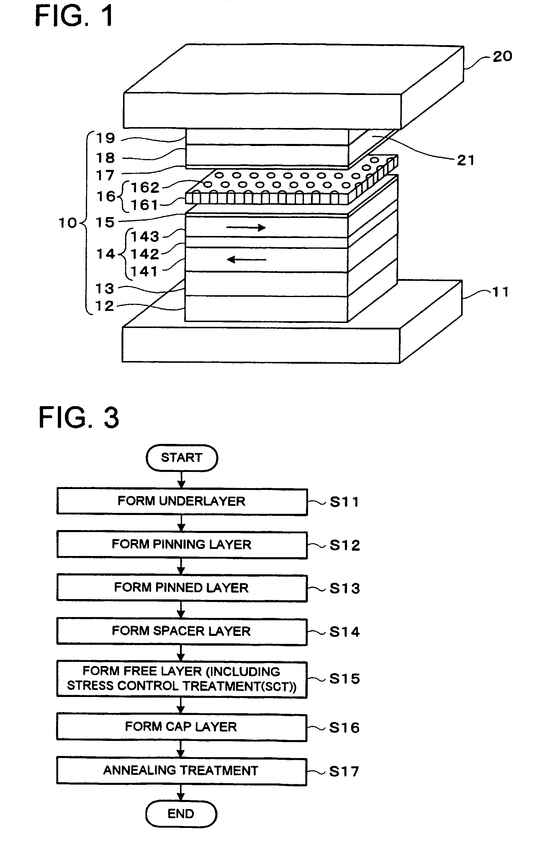
[0035]FIG. 1 is a perspective view showing a magnetoresistive effect element (CCP-CPP element) according to a first embodiment. FIG. 1 and the other drawings are all schematic views, and the ratio of the film thicknesses in the drawings and the ratio of the actual film thicknesses do not always coincide with each other.
[0036]As shown in FIG. 1, the magnetoresistive effect element according to the present embodiment has a magnetoresistive effect film 10, and a lower electrode 11 and an upper electrode 20 which sandwich it from above and below, and is constructed on a substrate not shown.
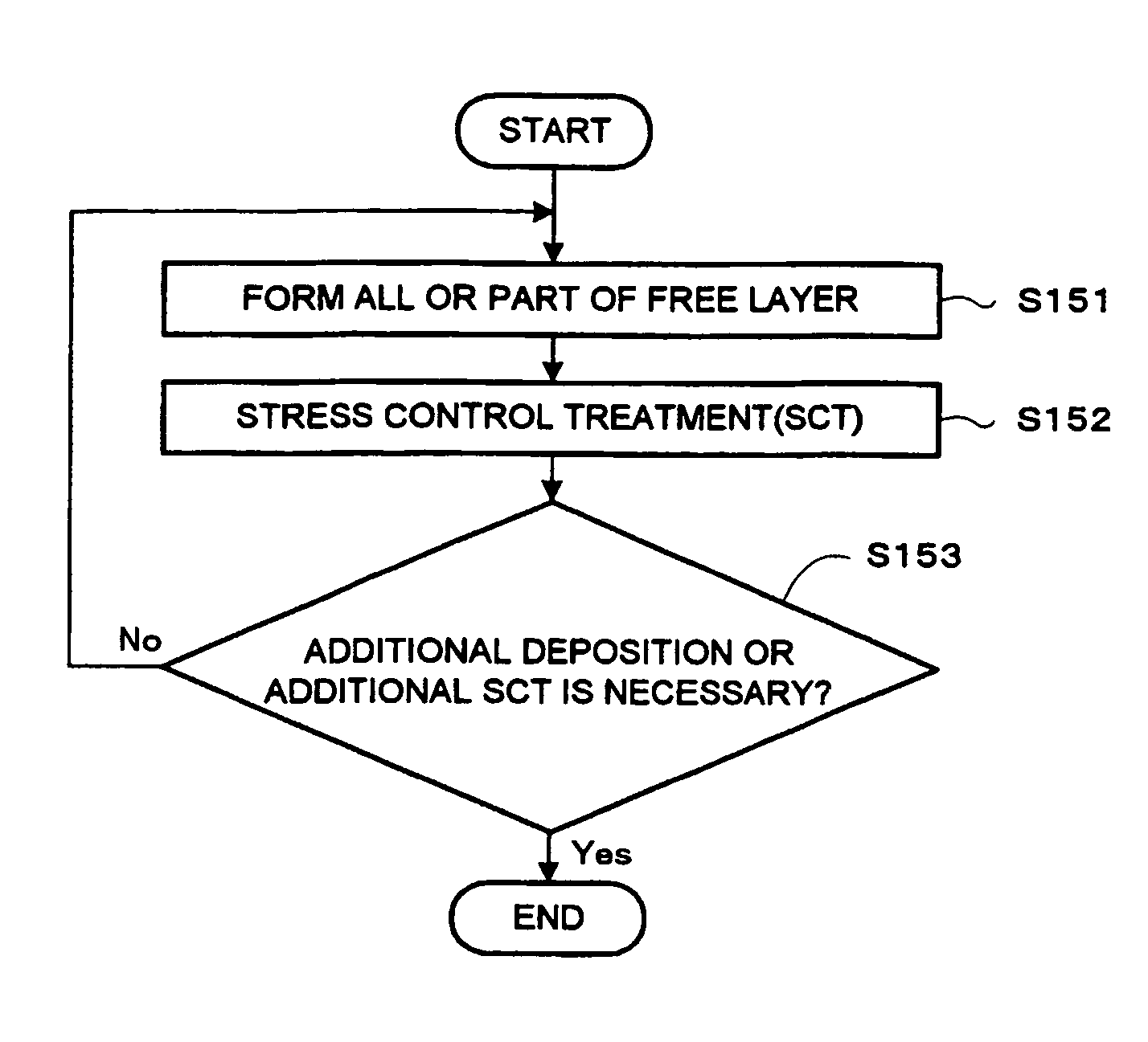
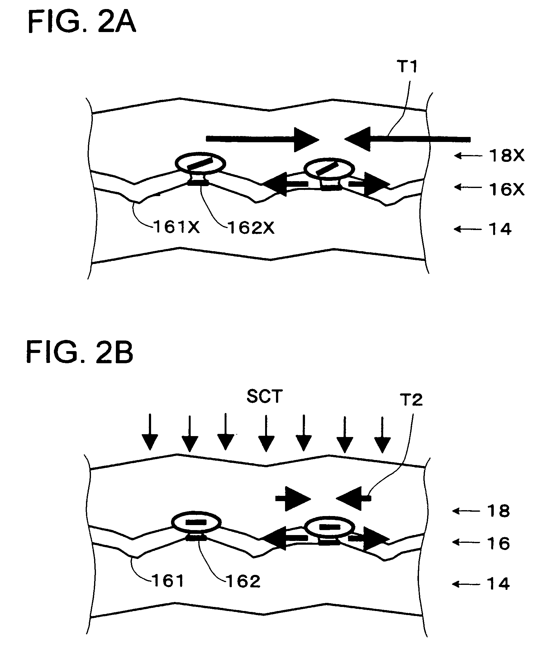
[0037]The magnetoresistive effect film 10 is constructed by a underlayer 12, a pinning layer 13, a pinned layer 14, a lower metal layer 15, a spacer layer (CCP-NOL) 16 (an insulating layer 161, a current path 162), an upper metal layer 17, a free layer 18, and a cap layer 19 being stacked in sequence. Among them, the pinned layer 14, the lower metal layer 15, the spacer layer 16, the upper metal layer...
example
[0236]Hereinafter, an example of the present invention will be described. The composition of the magnetoresistive effect film 10 according to the example of the present invention will be shown.[0237]The lower electrode 11[0238]The underlayer 12: Ta [5 nm] / Ru [2 nm][0239]The pinning layer 13: Pt50Mn50 [15 nm][0240]The pinned layer 14: Co90Fe10 [3.6 nm] / Ru [0.9 nm] / (Fe50Co50 [1 nm] / Cu [0.25 nm])×2 / Fe50CO50 [1 nm][0241]The metal layer 15: Cu [0.5 nm][0242]The spacer layer (CCP-NOL) 16: the insulating layer 161 of Al2O3 and the current path 162 of Cu (after depositing Al90Cu10 [1 nm], PIT / IAO treatment)[0243]The metal layer 17: Cu [0.25 nm][0244]The free layer 18: Co90Fe10 [1 nm] / Ni83Fe17 [0.7 nm] / SCT / Ni83Fe17 [1.8 nm] / SCT / Ni83Fe17 [1.8 nm] / SCT[0245]The cap layer 19: Cu [1 nm] / Ru [10 nm][0246]The upper electrode 20
[0247]The manufacture process of the free layer 18 will be described. The other processes are performed with the methods already described, and the explanation of them will be...
second embodiment
[0261]FIG. 9 is a perspective view showing a magnetoresistive effect element (CCP-CPP element) according to a second embodiment of the present invention. FIG. 10 is a flow chart showing a manufacture process of the magnetoresistive effect element according to the second embodiment of the present invention. The magnetoresistive effect element is a top type CCP-CPP element in which the pinned layer 14 is disposed above the free layer 18. Namely, SCT can be applied to not only a bottom type CCP-CPP element in which the pinned layer 14 is located below the free layer 18, but also to a top type CCP-CPP element.
[0262]In the case of a top-type spin-valve film, the layer requiring SCT is not the free layer 18 but the pinned layer 14. Since the crystal orientation of the magnetic layer which grows on the spacer layer 16 degrades, SCT to the magnetic film is required. In FIG. 9, the lower pinned layer 141 has a stress control part 21A.
[0263]The pinned layer 14 is composed of the lower pinned ...
PUM
| Property | Measurement | Unit |
|---|---|---|
| temperature | aaaaa | aaaaa |
| thickness | aaaaa | aaaaa |
| temperature | aaaaa | aaaaa |
Abstract
Description
Claims
Application Information