Eureka AIR delivers breakthrough ideas for toughest innovation challenges, trusted by R&D personnel around the world.

Tantalum amide precursors for deposition of tantalum nitride on a substrate

a precursor and tantalum nitride technology, applied in the direction of crystal growth process, polycrystalline material growth, group 5/15 element organic compounds, etc., can solve the problems of unstable source reagent, unsatisfactory candidate, and inhibit the integration of copper metallurgy in such microelectronic device applications, etc., to achieve rapid thermal processing

Inactive Publication Date: 2000-01-18
ENTEGRIS INC
View PDF26 Cites 318 Cited by
  • Summary
  • Abstract
  • Description
  • Claims
  • Application Information

AI Technical Summary

Benefits of technology

The tantalum nitride precursor composition thus may be provided as a liquid composition, which is delivered to a vaporizer to effect vaporization and formation of the tantalum nitride precursor vapor, with the vapor being transported to a deposition zone containing the substrate for the formation of the tantalum nitride material on the substrate. The formation of tantalum nitride material on the substrate may be carried out by a deposition process such as chemical vapor deposition, assisted chemical vapor deposition, ion implantation, molecular beam epitaxy and rapid thermal processing.

Problems solved by technology

Although CVD of Cu is gaining momentum in the semiconductor manufacturing industry, several problems still inhibit the integration of copper metallurgy in such microelectronic device applications.
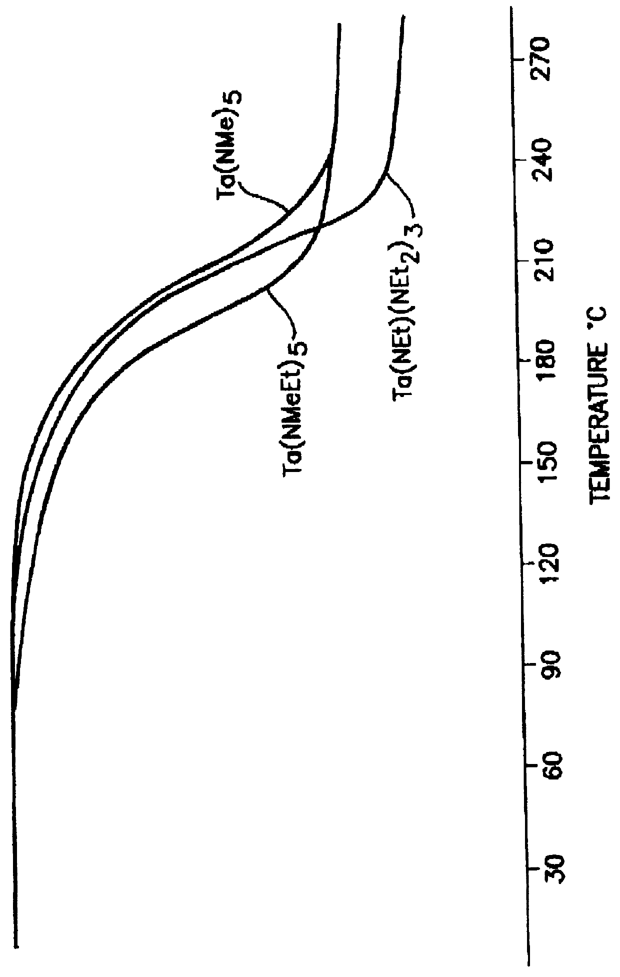
However, this source reagent is unstable to elevated temperature conditions, readily decomposing to a tantalum imide species, Ta(NEt)(NEt.sub.2).sub.3, upon heating, and thereby is an unsatisfactory candidate as a liquid source reagent for TaN barrier layer formation.
Apart from the hazards associated with handling a pyrophoric gas such as silane, the dual source reactor configuration required with such precursor species (TaCl.sub.5, Ta(NMe.sub.2).sub.5 and silane) also increases the cost and complexity of the semiconductor manufacturing operation.

Method used


Image

  • Tantalum amide precursors for deposition of tantalum nitride on a substrate
  • Tantalum amide precursors for deposition of tantalum nitride on a substrate
  • Tantalum amide precursors for deposition of tantalum nitride on a substrate

Examples


Embodiment Construction

The present invention is based on the discovery of highly advantageous Ta and Ti source reagents, including Ta source reagents useful for forming Ta-based barrier layers on substrates such as microelectronic device structures for applications such as copper metallization of semiconductor device structures.

The Ta source reagents of the invention include TaN source reagents including Ta amides, as well as single source precursors that are advantageous for the deposition of TaSiN and TiSiN in which silicon is incorporated at the molecular level into the precursor.

In the provision of Ta amide precursors for the formation of TaN barrier layers, useful precursors include tantalum amide precursor compositions comprising at least one tantalum amide species selected from the group consisting of:

(i) tethered amine tantalum complexes of the formula: ##STR7##

wherein:

X is 2 or 3;

each of R.sub.1 -R.sub.5 is independently selected from the group consisting of H, C.sub.1 -C.sub.4 alkyl, aryl (e.g, ...


PUM

PropertyMeasurementUnit
melting pointaaaaaaaaaa

Abstract

Tantalum and titanium source reagents are described, including tantalum amide and tantalum silicon nitride precursors for the deposition of tantalum nitride material on a substrate by processes such as chemical vapor deposition, assisted chemical vapor deposition, ion implantation, molecular beam epitaxy and rapid thermal processing. The precursors may be employed to form diffusion barrier layers on microlectronic device structures enabling the use of copper metallization and ferroelectric thin films in device construction.

Description

1. Field of the InventionThe present invention relates to Ta and Ti precursors useful in the formation of a Ta-based or Ti-based material on a substrate, and includes tantalum amide precursors for formation of tantalum nitride on a substrate, and methods of use of such precursors for forming TaN material, e.g., thin film layers of TaN, on a substrate. The invention also contemplates single source compounds for the formation of TaSiN or TiSiN material on a substrate.2. Description of the Related ArtCopper is of great interest for use in metallization of VLSI microelectronic devices because of its low resistivity, low contact resistance, and ability to enhance device performance (relative to aluminum metallization) via reduction of RC time delays thereby producing faster microelectronic devices. Copper CVD processes which are suitable for large-scale manufacturing and the conformal filling of high aspect ratio inter-level vias in high density integrated circuits are extremely valuable...

Claims


Application Information

Patent Timeline
Patent Type & Authority Patents(United States)
IPC IPC(8): C07F9/00C23C16/18C30B25/02C23C16/34C30B25/10C23C16/30C23C14/06C23C14/48
CPCC07F9/005C23C16/18C23C16/30C23C16/34C30B25/02C30B25/105C30B29/38C07F7/02
Inventor BHANDARI, GAUTAMBAUM, THOMAS H.
Owner ENTEGRIS INC
Why Eureka
Eureka Blog
Learn More