Apparatus for imaging using an array of lenses

a technology of arrays of lenses and cameras, applied in the field of digital imaging and photographic camera technology, can solve the problems of high cost of such an apparatus, inability to shrink optical cameras to dimensions compatible with nanodevice applications, and imaging devices are inherently more complex than sensors

Active Publication Date: 2011-12-13
NANOLIGHT TECH
View PDF5 Cites 195 Cited by
  • Summary
  • Abstract
  • Description
  • Claims
  • Application Information

AI Technical Summary

Benefits of technology

[0022]All functional elements of the imaging apparatus and / or camera as described above can be made out of various kind of materials and in one implementation be made out of flexible material. The optical elements may be arranged cylindrically as on a flexible tape, or spherically to obtain wide angle views. It can also be used for wide angle view detection by curving the sensor array in a 2-dimensional fashion combined with stitching the information together thereby producing up to 360 degree panoramic imaging.

Problems solved by technology

This construction necessitate the use of a relatively large lens system which in turn means that the cost for such an apparatus is high as well as the actual size of the apparatus will be dictated by the lens system employed.
This makes it impossible to shrink optical cameras to dimensions that will be compatible with nanodevice applications such as guiding micron sized autonomous systems for microsurgery, surveillance, reconnaissance and other future converging technologies.
Imaging devices are inherently more complex than sensors and thus present unique problems as compared to nano or micron-sized,transducers that sense various forms of energy including simple light detectors.
If one would have one lens for many pixel elements when trying to make such imaging systems smaller, one would be hindered from obtaining good imaging capability due to diffraction limits.
Thus physical laws limit the usefulness e.g. in millimeter sized imaging devices having rather low resolution.

Method used


Image

  • Apparatus for imaging using an array of lenses
  • Apparatus for imaging using an array of lenses
  • Apparatus for imaging using an array of lenses

Examples


Embodiment Construction

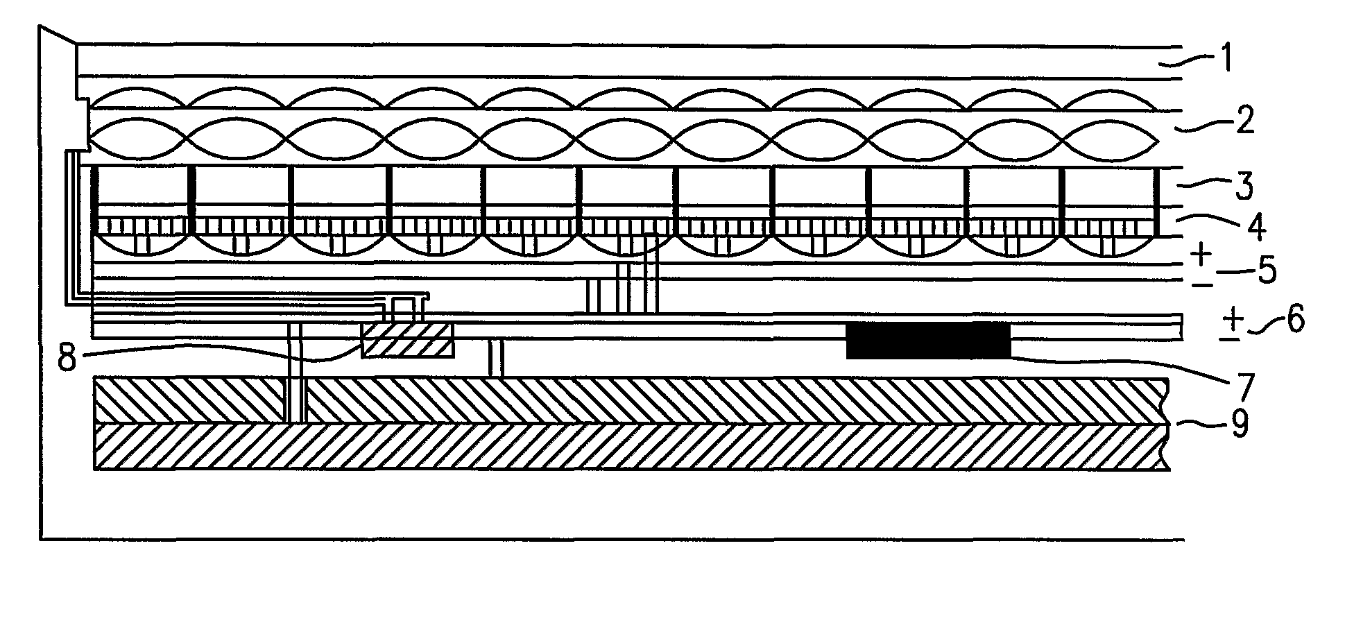
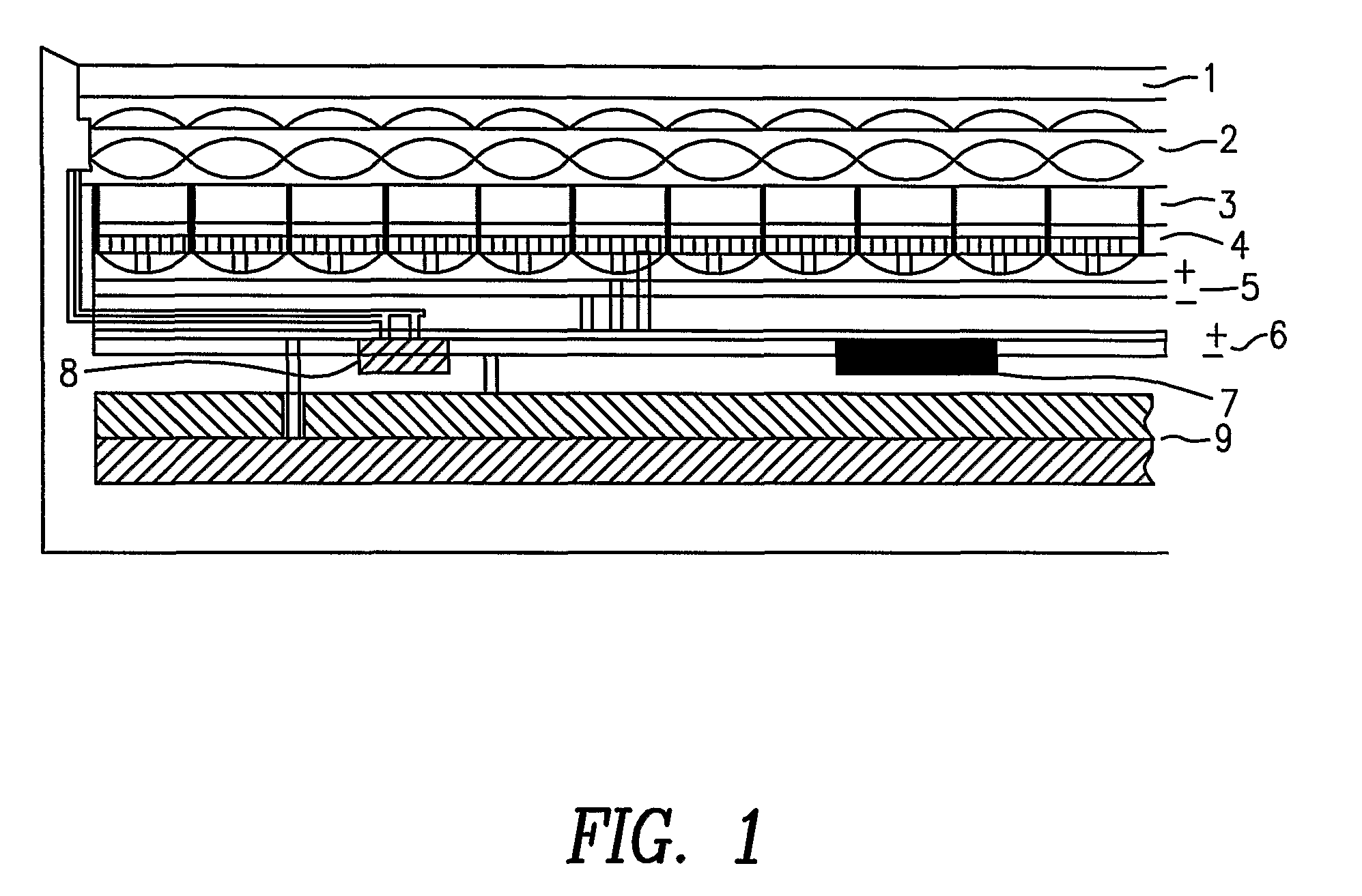
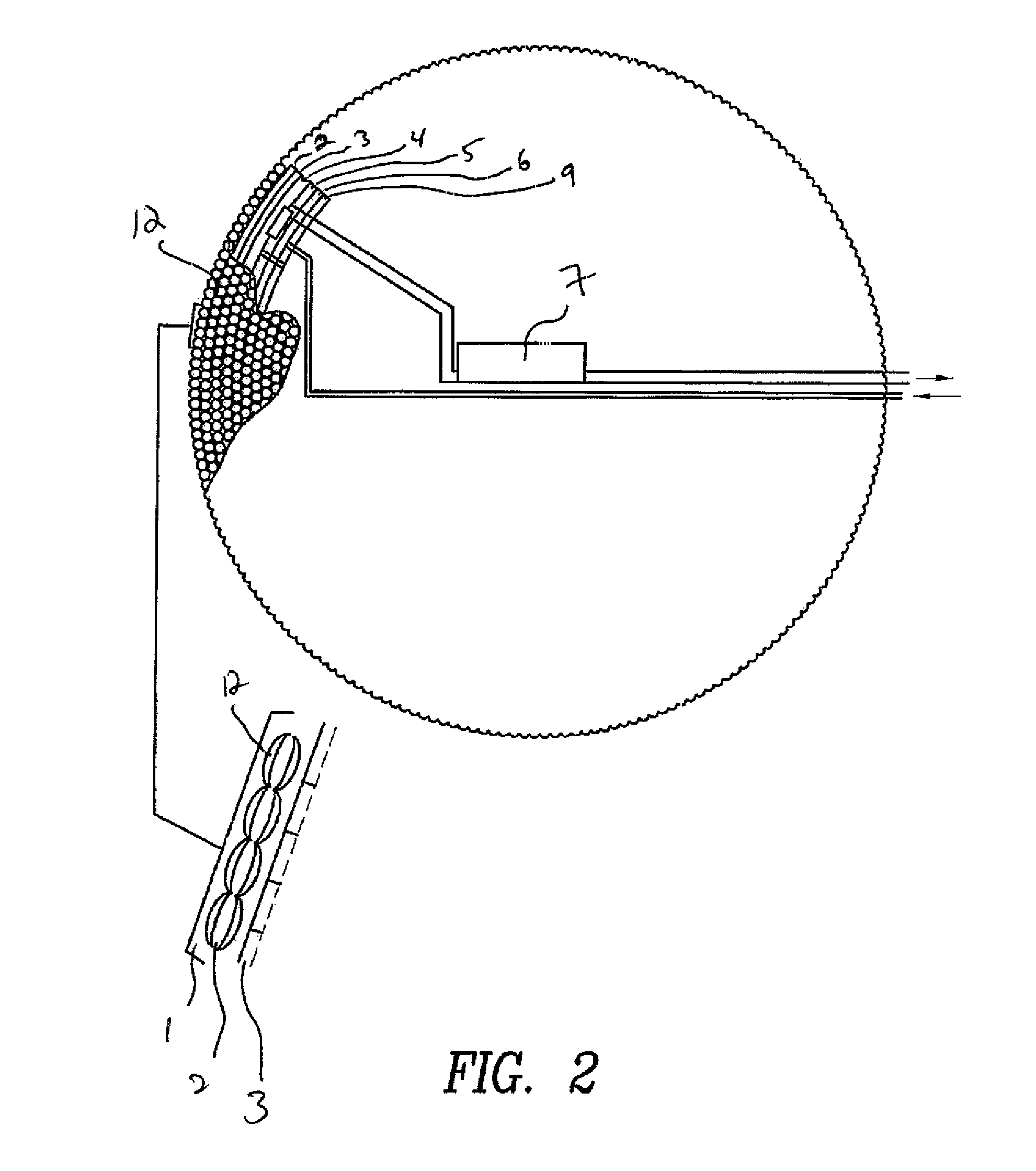
[0043]An extraordinarily small imaging system / camera characterized by having a high resolution through nanofabrication and image processing in which the fabrication of layered elements can be applied to a flat or flexible base such as tape.

[0044]Nano / macrosized optical elements 12 arranged in an array format 2 with more than one pixel per nano-sized optical element will become an imaging device itself rather than a light sensor (see FIG. 1).

[0045]Since an array is used, each element being at a different point gathers slightly different overlapping information, processing such information by interpolation, and / or interferometrically, one can obtain an image with much higher resolution than each of these multiple elements would be capable of individually and without a larger aperture and focal length single lens. Under most conditions focusing will be unnecessary due to extreme depth of field but may be controlled as outlined below or by the program algorithms used.

[0046]Since each of...


PUM

PropertyMeasurementUnit
focal lengthaaaaaaaaaa
volumeaaaaaaaaaa

Abstract

An imaging system / camera consisting of multiple nano-sized optical elements arranged in an array format with more than one pixel per optical element will have a higher resolution than each element would be capable of individually, since each element being at a different point gathers slightly different overlapping information. Hence by processing such information one can obtain a clear image. Furthermore multiple information from sectors of an array of sensors can be processed to obtain 3-D, stereotypic and panoramic imaging and may be connected to each other allowing seeing around obstacles as well as enabling full 3-D tracking and / or metric determination of an unknown object. Color / spectroscopic imaging can be achieved by utilizing equally sized lenses and multi-wavelength sensing layers below the lenses. However, color / spectroscopic imaging and / or spectroscopy can be achieved by taking advantage of unique optical properties of nano-scaled lenses accepting various wavelengths below their diffraction limits.

Description

BACKGROUND OF INVENTION[0001]1. Field of Invention[0002]The invention relates mainly to digital imaging and photographic camera technology for detection of electromagnetic radiation.[0003]2. Other areas[0004]Other potential areas can be systems for digital photography and imaging, medical, research, industrial, civil and military surveillance, monitoring and automatic sensor function. The electromagnetic radiation to be detected can be of all kinds including but not limited to ordinary visible light, UV-light, IR-light and THz-radiation.[0005]Examples of applications for this technology:[0006]Motion Detectors with Imaging Capability[0007]Biological, Medical and Surgical Imaging[0008]Cell and Sub-cellular Imaging[0009]Implanted Devices[0010]Micron and Nanosized Vehicles for guidance and reconnaissance[0011]Imaging from Aircraft, Space Vehicles or Rovers, particularly small robotically controlled vehicles, such as Micro or Nano[0012]Unmanned Aerial Vehicle (MUAV, NUAV)[0013]Ultralight...

Claims


Application Information

Patent Timeline
Patent Type & Authority Patents(United States)
IPC IPC(8): H04N5/335H04N5/225G01J3/02G02B3/00G02FG03B33/14G03F7/00H04N5/369
CPCG01J3/02G01J3/0208G01J3/0256G02B3/0056G02B3/0062G03B33/14H04N3/1593H04N5/23238H04N5/369H04N5/3696G02B3/0006H04N23/60H04N23/698H04N25/41H04N25/70
Inventor ADAMO, THOMAS J.MONTELIUS, LARS
Owner NANOLIGHT TECH
Why Eureka
Try Eureka