Error correction for digital systems

a technology of error correction and digital systems, applied in the direction of coding, instruments, code conversion, etc., can solve the problems of low manufacturing yield or performance of individual components, chip-bonding problems, oxidising connector contacts, etc., and achieve the effect of minimal design and implementation costs

Inactive Publication Date: 2012-01-03
IBM CORP
View PDF4 Cites 24 Cited by
  • Summary
  • Abstract
  • Description
  • Claims
  • Application Information

AI Technical Summary

Benefits of technology

[0008]It is an aim of the invention to improve the efficiency of sequential multiple-bit error correction. It is most suitable for situations where gradual degradation is the dominant mechanism, rather than simultaneous burst errors across multiple data bits. Another application is in situations where the manufacturing yield or performance of individual components is low, for example, due to interconnect problems.
[0009]It is a further aim of the invention to protect against gradual degradation of data lines and communication paths such as are frequently employed in chip-to-chip or system-to-system communications buses. Examples include oxidising connector contacts, chip-bonding problems and mechanical damage to connectors or cables.
[0024]Additional complexity is added to the system in a modular manner. The modules are scaleable and take advantage of present modular design philosophies together with cheap silicon. Design and implementation costs may be minimal and incorporated into a standard product range with no functional dependency on enabled devices at the other end of the communications bus.

Problems solved by technology

Another application is in situations where the manufacturing yield or performance of individual components is low, for example, due to interconnect problems.
Examples include oxidising connector contacts, chip-bonding problems and mechanical damage to connectors or cables.

Method used


Image

  • Error correction for digital systems
  • Error correction for digital systems
  • Error correction for digital systems

Examples


Embodiment Construction

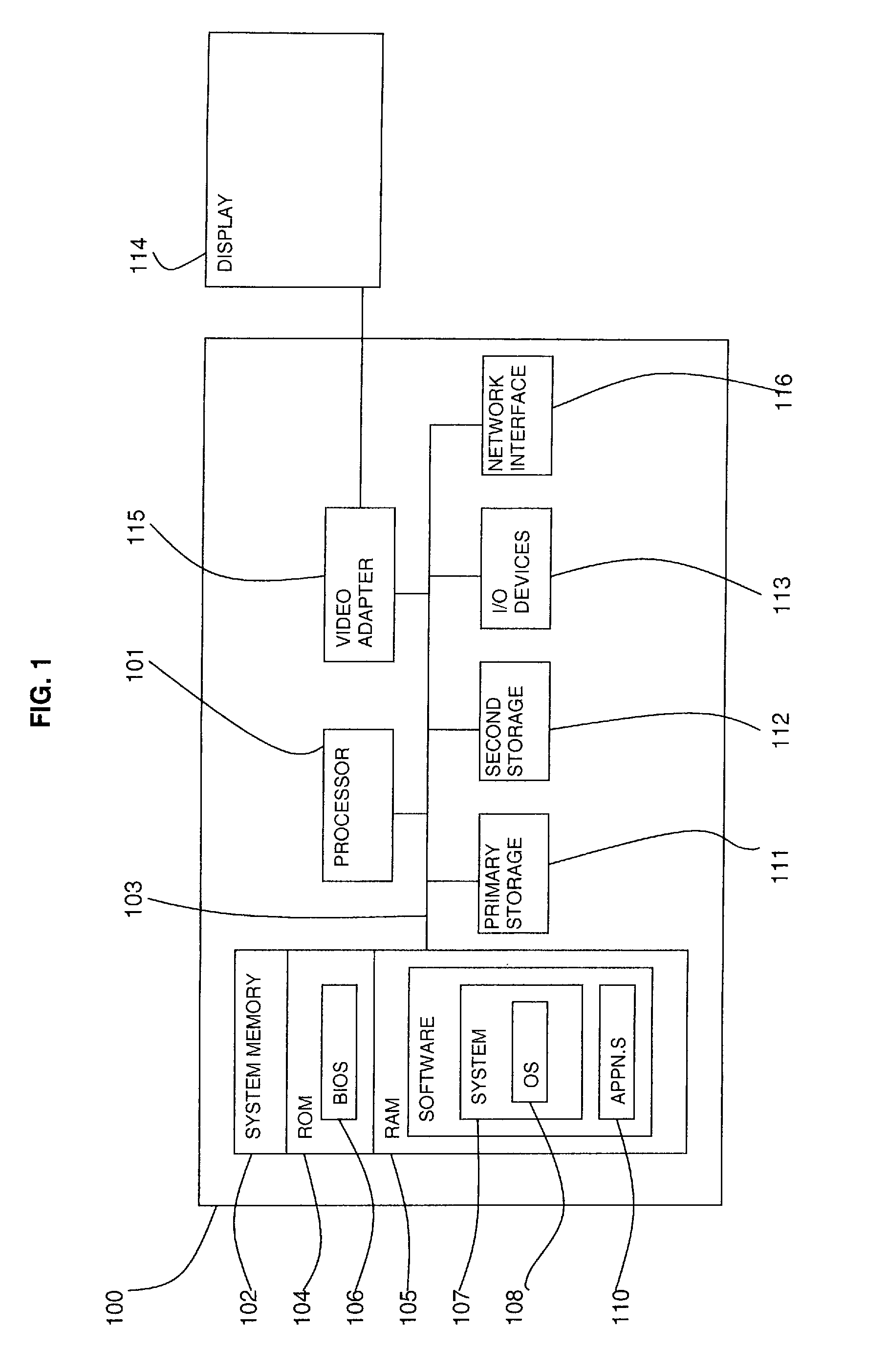
[0031]Referring to FIG. 1, a known data processing system 100 is shown in which the described error correction may be used in multiple different contexts. The data processing system 100 is suitable for storing and / or executing program code including at least one processor 101 coupled directly or indirectly to memory elements through a bus system 103. The memory elements can include local memory employed during actual execution of the program code, bulk storage, and cache memories which provide temporary storage of at least some program code in order to reduce the number of times code must be retrieved from bulk storage during execution.

[0032]The memory elements may include system memory 102 in the form of read only memory (ROM) 104 and random access memory (RAM) 105. A basic input / output system (BIOS) 106 may be stored in ROM 104. System software 107 may be stored in RAM 105 including operating system software 108. Software applications 110 may also be stored in RAM 105.

[0033]The sy...


PUM


Abstract

An interface system is provided between a source component (210) and a destination component (220) having multiple parallel lines for transmitting data or parity bits (231-234, 251-253) and one or more spare lines (241-243). An error detection means (222) identifies one or more faulty lines. A mapping means (228) re-routes data or parity from a faulty line to a spare line. A communication link (208) is provided for communicating the re-routing between the source component (210) and the destination component (220). The error detection and mapping can be repeated to detect and re-route sequential multiple-bit line errors using additional spare lines (241-243).

Description

CROSS REFERENCES TO RELATED APPLICATIONS[0001]This application is related to GB Patent Application No. 0612892.0, filed Jun. 29, 2006.FIELD OF THE INVENTION[0002]This invention relates to the field of error correction for digital systems. In particular, it relates to error correction in parallel data connections at chip, package, card, or system level.BACKGROUND OF THE INVENTION[0003]Error correction has been explored to secure the integrity of digital information transmitted from one device to another. Known algorithms generally apply additional parity bits to message data bits in order to provide error detection and / or correction. Parity methods are known for detecting and correcting a single error bit in parallel data transfer. However, methods for detection and correction of double or multiple-bit errors tend to increase the number of data bits required substantially.[0004]Memory errors appear for two reasons. One reason is a fault in the transport of the data from the memory to...

Claims


Application Information

Patent Timeline
Patent Type & Authority Patents(United States)
IPC IPC(8): G06F11/20
CPCG06F11/2007H04L1/0061H04L1/22H03M13/09
Inventor MACIVER, MARK ALASDAIRMACKENZIE, JAMES KEITH
Owner IBM CORP
Why Eureka
Try Eureka