Organic devices, organic electroluminescent devices and organic solar cells

a solar cell and electroluminescent technology, applied in the direction of instruments, discharge tubes luminescnet screens, natural mineral layered products, etc., can solve the problems of insufficient light transmissivity and limited thickness of the devi

Active Publication Date: 2012-01-24
MITSUBISHI HEAVY IND LTD +1
View PDF21 Cites 36 Cited by
  • Summary
  • Abstract
  • Description
  • Claims
  • Application Information

AI Technical Summary

Benefits of technology

[0021]The charge transfer complex-contained layer can be an interfacial layer disposed between two layers each consisting of hole-transporting molecules having different molecular structures for reducing the barrier height of the hole transfer between the two layers.
[0030]In an embodiment, an organic device is provided, having a layer structure on a substrate in the following deposition sequence: (A) an anode, (B) a layer structure mainly consisting of organic compounds (C) a radical anion-contained layer in which an organic electron-transporting molecule is in a state of radical anions generated by a radical anion generation means, (D) a cathode-adjacent layer consisting of a mixture of MoO3 and an organic hole-transporting molecule, and (E) a cathode layer, wherein the laminated layer of (C) and (D) works as “hole current-electron current conversion layer” as well as “damage reduction layer” to reduce the damage induced during the electrode deposition process.
[0031]In an embodiment, an organic electroluminescent device is a MPE organic EL device containing multiple light emissive units, wherein a layer structure on a substrate is provided in the following deposition sequence: (A) an anode, (B) a layer structure mainly consisting of organic compounds (C) a radical anion-contained layer in which an organic electron-transporting molecule is in a state of radical anions generated by radical anion generation means, (D) a cathode-adjacent layer consisting of a mixture of MoO3 and an organic hole-transporting molecule, and (E) a cathode layer, wherein the laminated layer of (C) and (D) works as “hole current-electron current conversion layer” as well as “damage reduction layer” to reduce the damage induced during the electrode deposition process.

Problems solved by technology

However, V2O5 is categorized as a deleterious substance, and further, does not have a sufficient light transmissivity.
However, according to the Reference 7, a layer of molybdenum oxide has only a transmittance of 10% at a thickness of 2,150 Å, and thus its thickness is limited due to the reduced light transmissivity which is considered to be resulting from oxygen desorption during the sputtering process.

Method used


Image

  • Organic devices, organic electroluminescent devices and organic solar cells
  • Organic devices, organic electroluminescent devices and organic solar cells
  • Organic devices, organic electroluminescent devices and organic solar cells

Examples


example 1

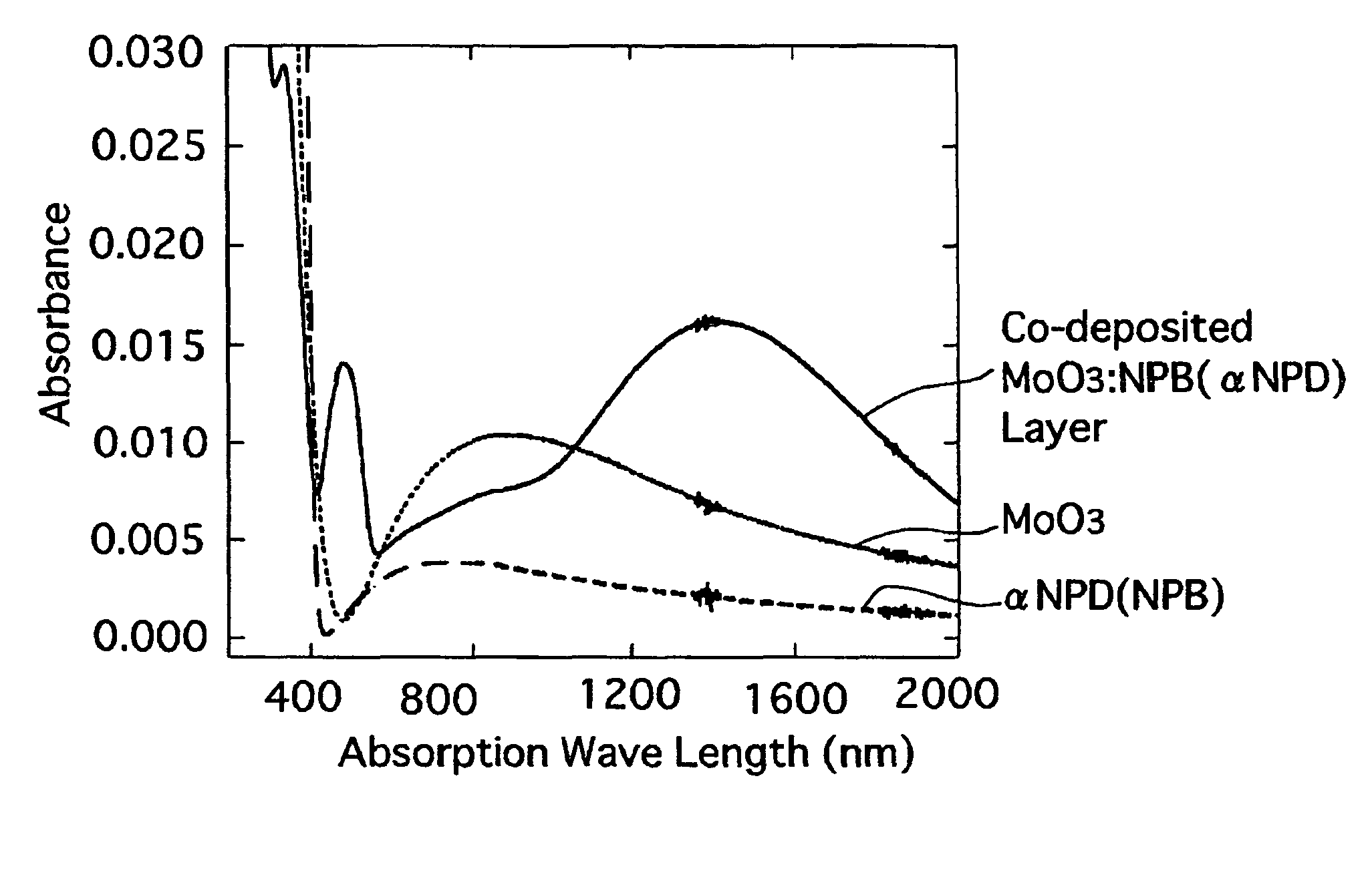
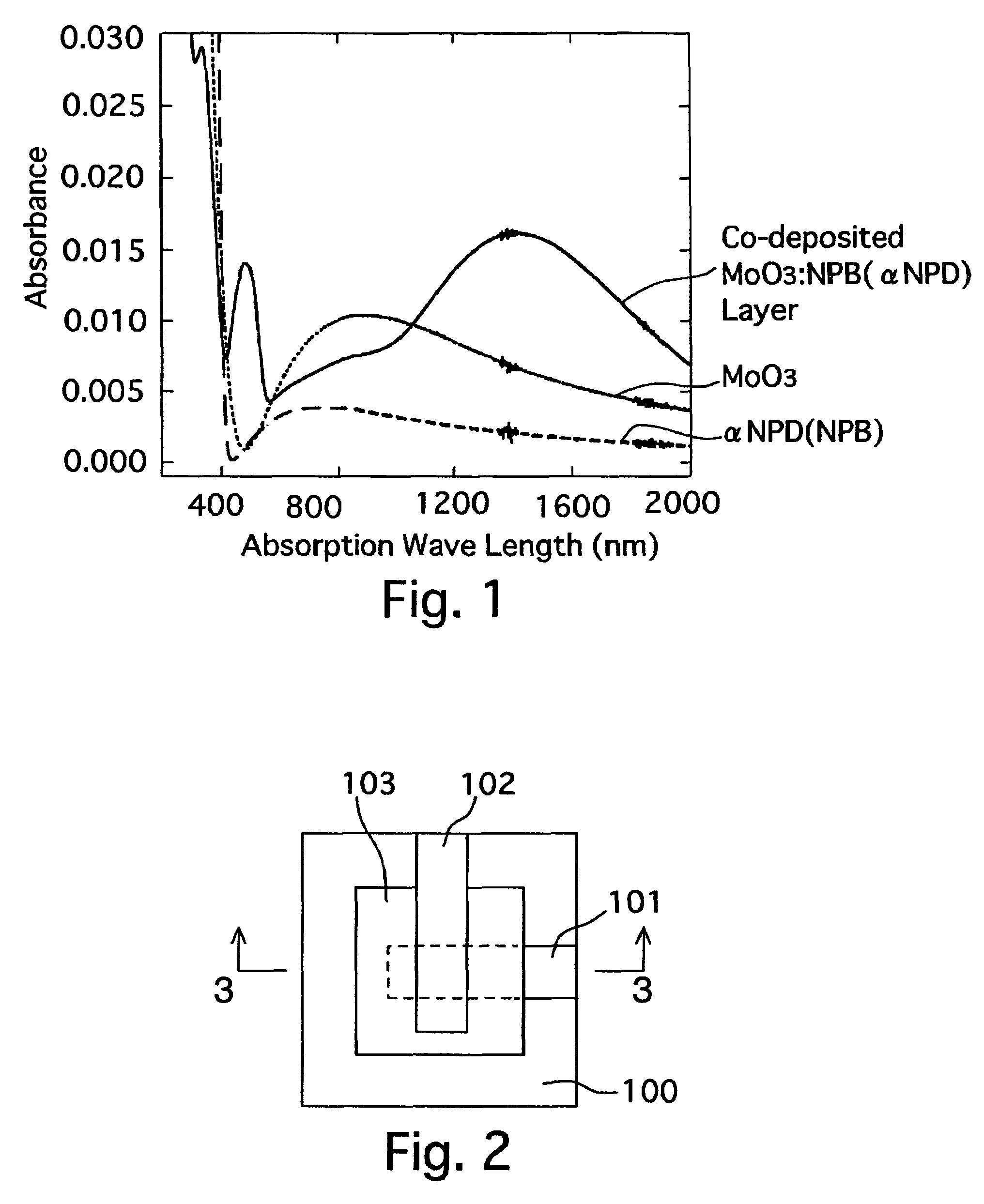
[0070]In Example 1, an absorption spectrum and its absorbance value (at layer thickness of 10 nm) was determined for each of the layers which are the main constituents of the present invention, i.e., a vacuum-deposited layer of MoO3 (molybdenum trioxide), a vacuum-deposited layer of α-NPD (also abbreviated to NPB) as an organic hole-transporting compound and a co-deposited layer of MoO3 and α-NPD (MoO3:α-NPD=5:1, molar ratio).

[0071]Measurement results are plotted in FIG. 1. As can be understood from FIG. 1, prominent peaks could be observed in the region of around 500 nm and around 1,400 nm for the co-deposited layer of MoO3 and α-NPD. These peaks could not be observed for each of the single layer of MoO3 and the single layer of α-NPD, and clearly indicates the formation of a charge transfer complex as a result of the oxidation reduction reaction between these two substances, i.e., formation of radical cations (NPB+) of NPB as the organic hole-transporting compound.

example 2

[0072]In Example 2, the measurement of the resistivity of MoO3 or the mixture layer, prepared by co-deposition of MoO3 and the organic hole-transporting compound, was carried out while comparing with the results from V2O5 or the mixture layer, also prepared by co-deposition of V2O5 and the organic hole-transporting compound, having been already disclosed in the prior invention by the inventors. The measurement of the resistivity (unit: Ωcm) was carried out with the following two methods depending on the values (range) of the resistivity of the substance to be tested (hereinafter, test substance).

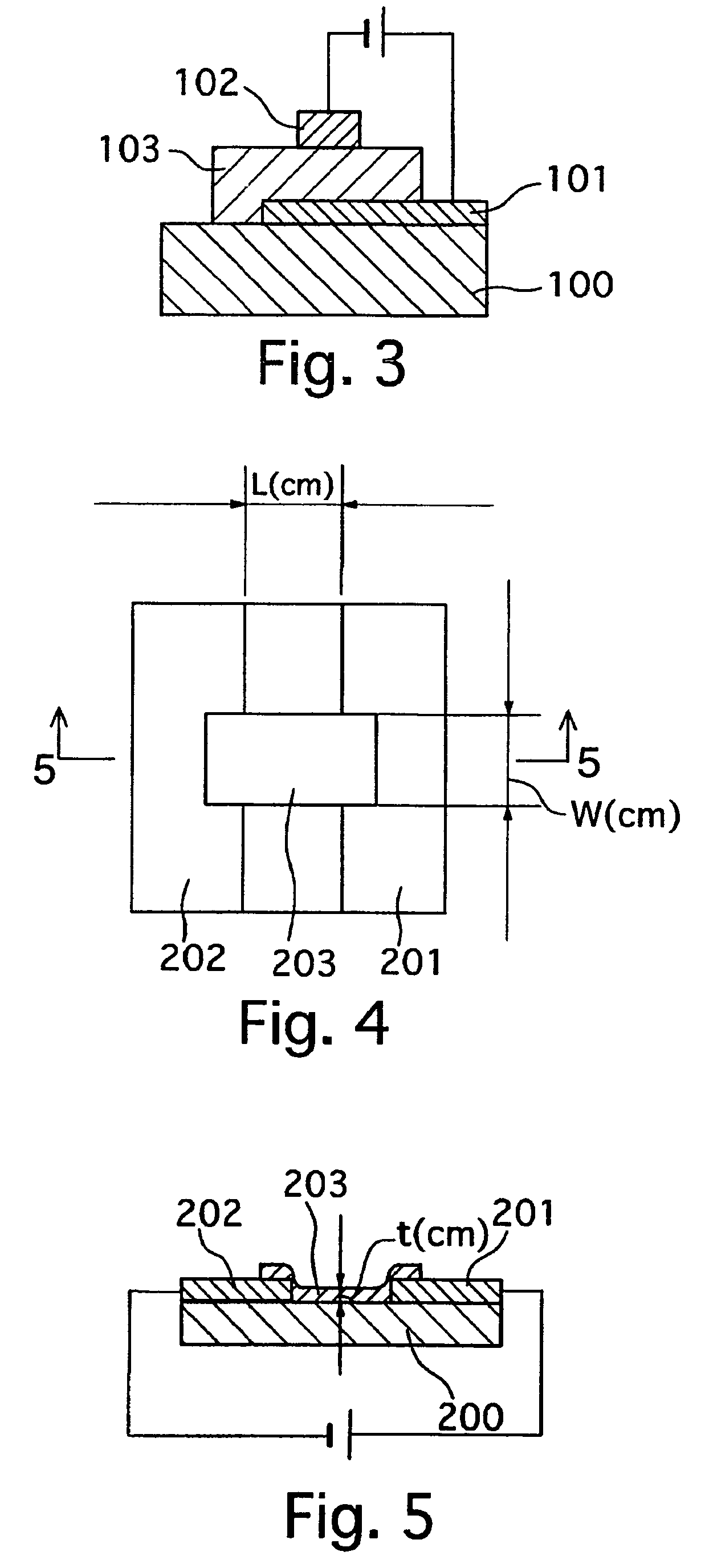
[0073]The first measurement method (sandwich method) is a method suitable for the substances having a relatively high resistivity. The measurement of the resistivity is carried out by sandwiching a deposited thin layer 103 of the test substance in between two electrodes 101 and 102 (the resistivity evaluation device having a sandwich structure shown in FIGS. 2 and 3). The resistivity is calc...

example 3

[0097]In Example 3, the measurements of the transmittance (at 1000 Å thick=100 nm thick) in the visible light wave length region were conducted for the main constituents of the present invention, i.e., “MoO3 deposition layer” and “co-deposited layer of MoO3 and α-NPD”, and for the “V2O5 deposition layer” which can function similar way in the organic devices.

[0098]Measurement results are plotted in FIG. 8. As can be understood from FIG. 8, it has been found that the “MoO3 deposition layer” and “co-deposited layer of MoO3 and α-NPD” of the present invention can exhibit a higher transmittance in a substantially full range of the visible light region in comparison with the “V2O5 deposition layer”. Accordingly, it can be appreciated that the above layers of the present invention can be more advantageously used as a layer for an organic device such as an organic EL element and an organic solar cell.

[0099]Hereinafter, the organic EL element and an organic solar cell will be specifically de...


PUM

PropertyMeasurementUnit
DC voltageaaaaaaaaaa
external quantum efficiencyaaaaaaaaaa
luminanceaaaaaaaaaa

Abstract

An organic device, including an organic compound having charge-transporting ability (i.e., transporting holes and / or electrons) and / or including organic light emissive molecules capable of emitting at least one of fluorescent light or phosphorescent light, has a charge transfer complex-contained layer including a charge transfer complex formed upon contact of an organic hole-transporting compound and molybdenum trioxide via a manner of lamination or mixing thereof, so that the organic hole-transporting compound is in a state of radical cation (i.e., positively charged species) in the charge transfer complex-contained layer.

Description

CROSS REFERENCE TO RELATED APPLICATION[0001]The present application is related to and claims priority of the following co-pending application, namely, Japanese Patent Application No. 2004-202266 filed on Jul. 8, 2004.BACKGROUND OF THE INVENTION[0002]1. Field of the Invention[0003]The present invention relates to an organic device, an organic electroluminescent device (hereinafter, abbreviated as an “organic EL device”) and an organic solar cell each using an organic charge-transporting compound.[0004]2. Background Art[0005]In recent years, organic semiconductors and organic conductive materials have been actively studied, and in particular, remarkable process has been achieved in organic EL devices which are light emissive elements that use an organic semiconductor.[0006]In organic EL devices, Tang et al. have successfully discovered, with regard to the increase in efficiency of EL devices, that high luminance and high efficiency sufficient for practical use such as a luminance of 1...

Claims


Application Information

Patent Timeline
Patent Type & Authority Patents(United States)
IPC IPC(8): H01L31/00H01J1/62H01J63/04H01L51/30H01L51/50
CPCH01L51/0051H01L51/5056H01L51/0084H01L51/5088H01L51/506H01L51/5076H01L51/5215H01L51/5234H01L51/441H01L51/5221H01L51/0058H01L51/006H01L51/0078H01L51/0081H01L51/4206Y02E10/542Y02E10/549Y10S428/917H01L2251/5353H01L51/42H10K85/611H10K85/633H10K85/311H10K85/324H10K85/341H10K30/451H10K50/131H10K50/155H10K50/157H10K50/165H10K50/17H10K50/816H10K2102/321H05B33/26C09K11/06H10K30/81H10K50/15H10K50/82H10K50/828H10K85/626H10K30/00
Inventor KIDO, JUNJIMATSUMOTO, TOSHIONAKADA, TAKESHI
Owner MITSUBISHI HEAVY IND LTD
Why Eureka
Try Eureka