Flexible optical waveguide and process for its production

a technology process, applied in the field of flexible optical waveguides, can solve the problems of complex production steps and high production costs, and achieve the effects of excellent flexibility and heat resistance, excellent peel strength, and high adhesiveness

Inactive Publication Date: 2012-04-10
HITACHI CABLE +1
View PDF23 Cites 3 Cited by
  • Summary
  • Abstract
  • Description
  • Claims
  • Application Information

AI Technical Summary

Benefits of technology

[0009]Accordingly, it has been required to obtain a flexible optical waveguide which enables easy production of an opto-electronic hybrid integrated flexible module and which comprises an optical waveguide film formed directly on a substrate without using an adhesive or any other agent, and a process for its production in a simple and easy manner.
[0010]Under the above circumstances, an object to be solved by the present invention is to provide a flexible optical waveguide which makes it possible to directly form an optical waveguide film on a substrate without using an adhesive or any other agent and which is excellent in flexibility of the optical waveguide film, including the substrate, and adhesiveness between the substrate and the optical waveguide film; and a process for its production in a simple and easy manner.
[0016]With respect to the flexible optical waveguide of the present invention, a surface of a substrate, on which surface a lower cladding layer is to be formed, has an arithmetic average roughness (Ra) of 0.03 μm or higher by subjecting the surface of the substrate to physical treatment with a whetstone or chemical treatment with a corona discharge, and therefore, peel strength between the substrate and the lower cladding layer is high, for example, even if the flexible optical waveguide is continuously bent 100,000 times or more at ±90 degrees with a radius of 2 mm at room temperature, neither separation nor rupture occurs. This is because even if fine cracks are formed at the time of bending the flexible optical waveguide, the cracks thus formed do not spread largely due to high adhesiveness between the substrate and the lower cladding layer. Further, if a polyimide film is used as the substrate, because the polyimide film is excellent in flexibility and heat resistance, an opto-electronic hybrid integrated flexible module can be produced from the flexible optical waveguide.
[0017]In the process for producing a flexible optical waveguide according to the present invention, there is no need to include a step of forming an adhesive layer or any other layer between a substrate and a lower cladding layer, but there is only a need to include steps of subjecting a surface of the substrate, on which surface the lower cladding layer is to be formed, to physical treatment with a whetstone or chemical treatment with a corona discharge and then successively forming a lower cladding layer, a core layer, and an upper cladding layer on the surface of the substrate, and therefore, an optical waveguide film can be formed on the substrate in a simple and easy manner and production costs can remarkably be saved.

Problems solved by technology

However, in the opto-electronic hybrid integrated flexible module disclosed in Japanese Patent Laid-open Publication (Kokai) No. 2006-22317, epoxy resin films to be a lower cladding layer, a core layer, and an upper cladding layer of an optical waveguide need to be separately produced, and after these epoxy resin films are vacuum laminated onto a copper-clad polyimide substrate, the resulting film needs to be cured and a base film needs to be separated, and therefore, there is a problem that production steps become complicated and production costs becomes high.

Method used


Image

  • Flexible optical waveguide and process for its production
  • Flexible optical waveguide and process for its production
  • Flexible optical waveguide and process for its production

Examples


example 1

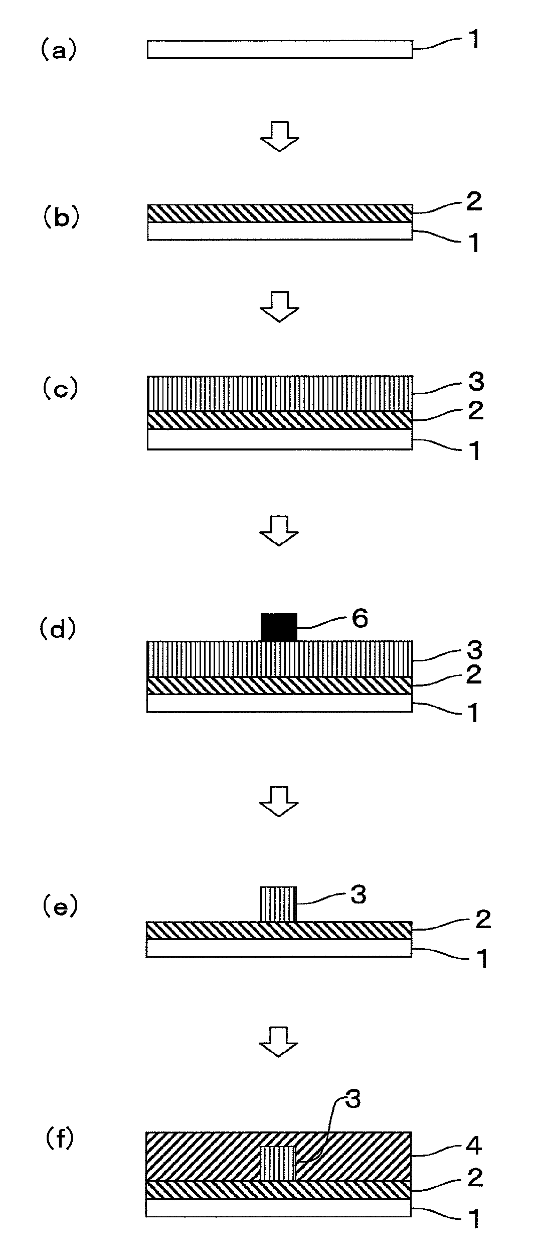
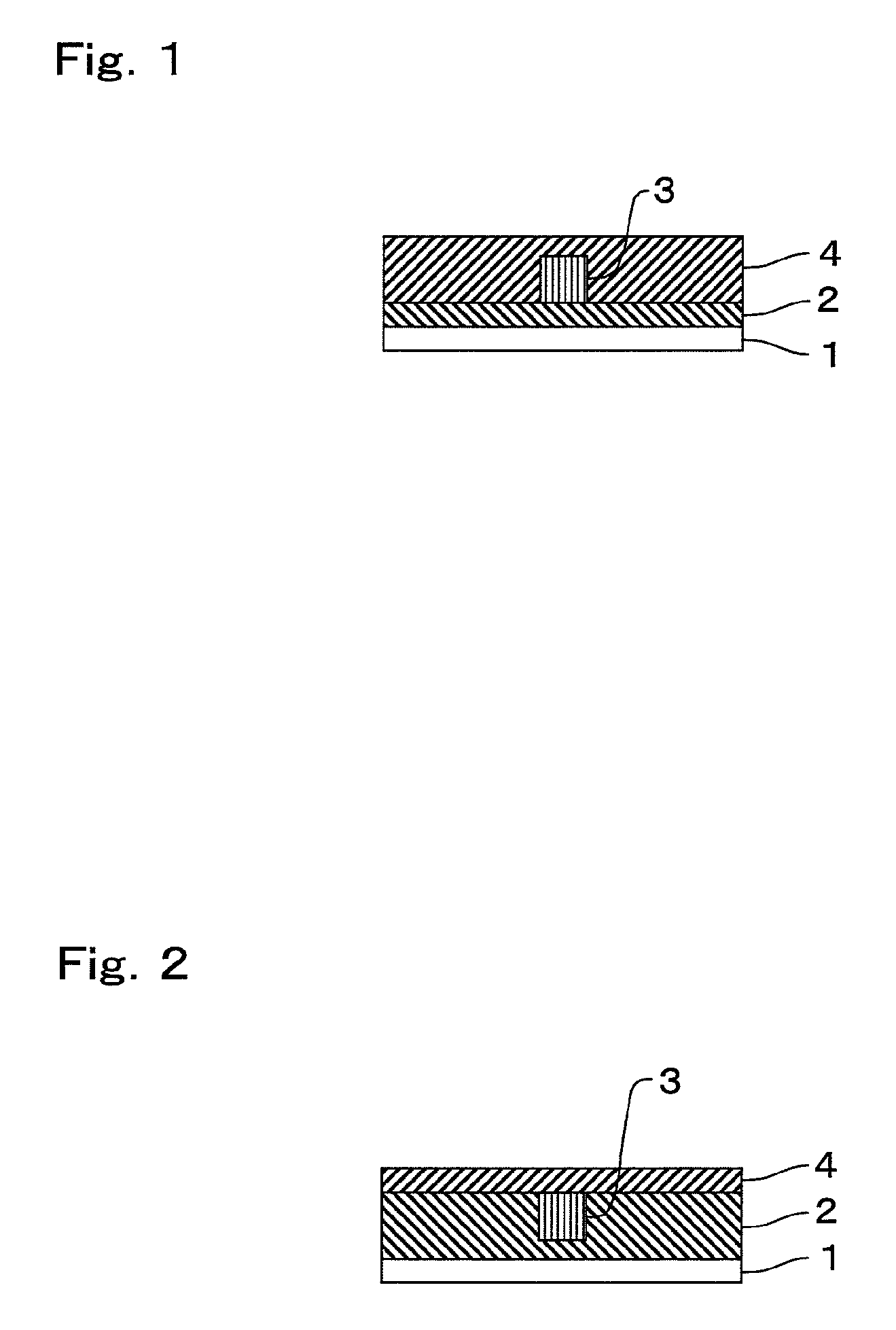
[0116]A polyimide film with a 8-μm thick copper circuit (product name: Kapton (registered trade name) H type, available from DuPont-Toray Co., Ltd.; the thickness thereof was 25 μm) was used as a substrate, and a surface of the substrate, which surface was reverse to the copper circuit, was subjected to physical treatment with a #3000 whetstone to form unevenness (the arithmetic average roughness (Ra) thereof was 0.08 μm) thereon.

[0117]The UV-curable epoxy resin (1) was coated as a cladding material on the surface of the substrate by spin coating technique and cured by carrying out ultraviolet irradiation at an illumination intensity of 10 mW / cm2 for 15 minutes, i.e., at an exposure energy of 9 J / cm2, by the use of an exposure apparatus (product name: MA-60F, available from Mikasa Co., Ltd.) with a high pressure mercury lamp as a light source to form a lower cladding layer composed of an epoxy type resin film having a thickness of 25 μm.

[0118]At this stage, peel strength between the...

example 2

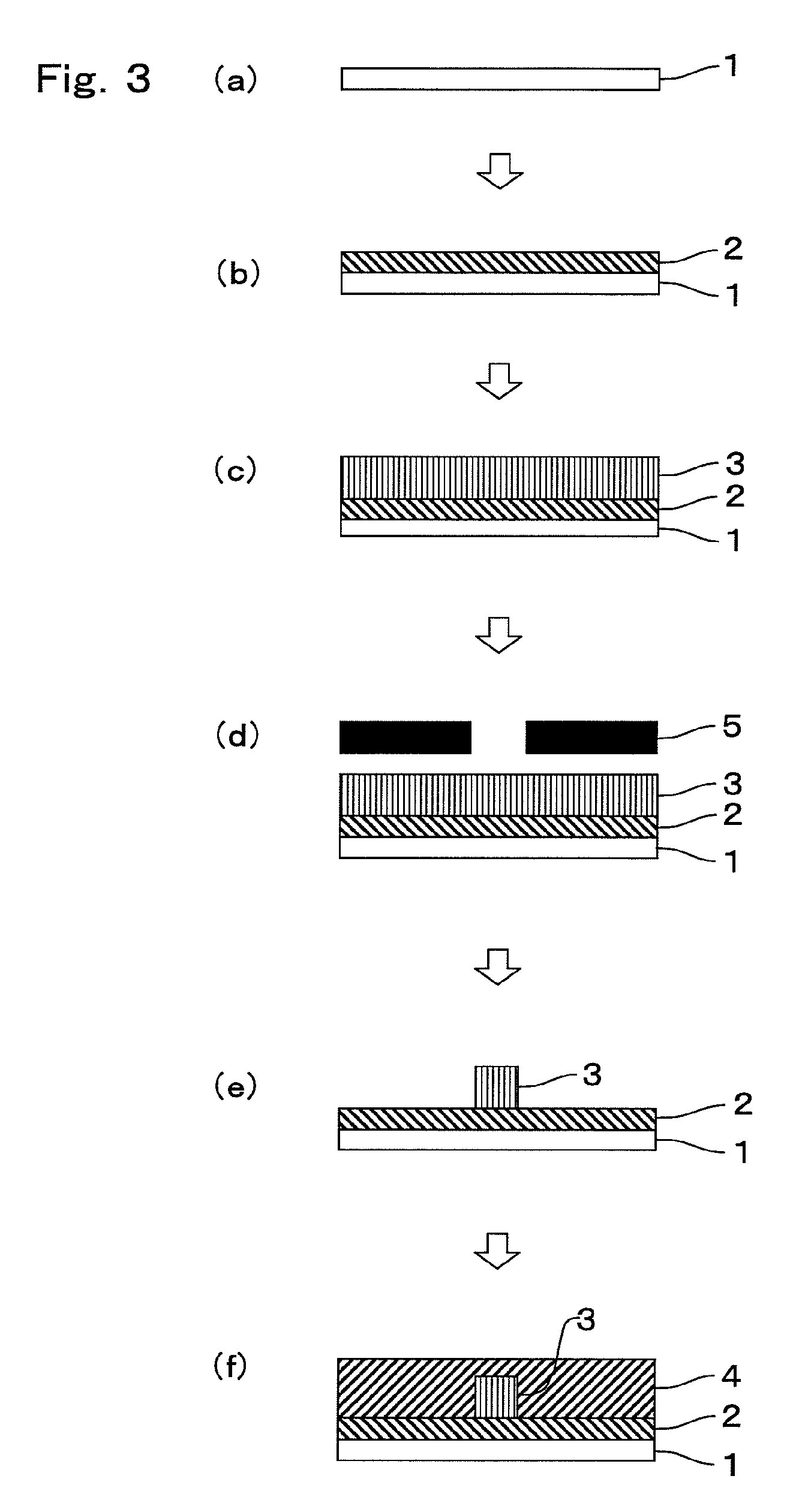
[0123]A flexible optical waveguide having a lower cladding layer, a core layer, and an upper cladding layer, all of which were composed of epoxy type resin films, on a substrate of a polyimide film was obtained in the same manner as described in Example 1, except that the #3000 whetstone was changed to a #6000 whetstone to form unevenness (the arithmetic average roughness (Ra) thereof was 0.06 μm) on a surface of the substrate, which surface was reverse to the copper circuit.

[0124]At the stage where the lower cladding layer was formed on the substrate, peel strength between the substrate and the lower cladding layer was measured using a tensile tester (product name: EZ-test-100N, available from Shimadzu Corporation) according to JIS K6894 8.6.3 and found to be 170 N / m, and it showed excellent adhesiveness.

[0125]When the waveguide loss of a flexible optical waveguide obtained in the same manner as described above was measured, it was 0.15 dB / cm. Further, even if a flexible optical wa...

example 3

[0126]A flexible optical waveguide having a lower cladding layer, a core layer, and an upper cladding layer, all of which were composed of epoxy type resin films, on a substrate composed of a polyimide film was obtained in the same manner as in Example 1, except that the #3000 whetstone was changed to a #8000 whetstone to form unevenness (the arithmetic average roughness (Ra) thereof was 0.05 μm) on a surface of the substrate, which surface was reverse to the copper circuit.

[0127]At the stage where the lower cladding layer was formed on the substrate, peel strength between the substrate and the lower cladding layer was measured using a tensile tester (product name: EZ-test-100N, available from Shimadzu Corporation) according to JIS K6894 8.6.3 and found to be 140 N / m, and it showed excellent adhesiveness.

[0128]When the waveguide loss of a flexible optical waveguide obtained in the same manner as described above was measured in the same manner, it was 0.15 dB / cm. Furthermore, even if...


PUM

PropertyMeasurementUnit
Raaaaaaaaaaa
peel strengthaaaaaaaaaa
Raaaaaaaaaaa

Abstract

The invention provides a flexible optical waveguide in which an optical waveguide film is directly formed on a substrate without using an adhesive and which is excellent in flexibility of the optical waveguide film, including the substrate, and excellent in adhesiveness between the substrate and the optical waveguide film, as well as a process for producing the flexible optical waveguide in a simple and easy manner. The flexible optical waveguide includes a lower cladding layer, a core layer, and an upper cladding layer successively formed on a substrate and a surface of the substrate, on which surface the lower cladding layer is to be formed, has an arithmetic average roughness (Ra) of 0.03 μm or higher. The flexible optical waveguide can be produced by subjecting a surface of the substrate, on which surface the lower cladding layer is to be formed, to physical treatment with a whetstone or chemical treatment with a corona discharge and then successively forming the lower cladding layer, the core layer, and the upper cladding layer on the surface of the substrate.

Description

BACKGROUND OF THE INVENTION[0001]1. Field of the Invention[0002]The invention relates to a flexible optical waveguide and a process for its production.[0003]2. Description of the Related Art[0004]Along with the practical applications of optical transmission systems, techniques relevant to optical waveguides as their basic components have drawn much attention. An optical waveguide has, typically, an embedded type structure in which a core layer having a high refractive index is surrounded with a cladding layer having a low refractive index, or a ridge type structure in which a core layer having a high refractive index is formed on a lower cladding layer having a low refractive index and an upper cladding layer is an air layer. Thus, light incoming to the optical waveguide is transmitted in the core layer while being reflected at the interface between the core layer and the cladding layers or at the interface between the core layer and the air layer.[0005]Recently, there have been dev...

Claims


Application Information

Patent Timeline
Patent Type & Authority Patents(United States)
IPC IPC(8): G02B6/10B32B38/00B05D5/12
CPCG02B6/10G02B6/138G02B6/02033Y10T156/1052H04M1/0274
Inventor USHIWATA, TAKAMIHIRANO, KOKITAJIRI, KOZOMAKINO, TOMOMI
Owner HITACHI CABLE
Why Eureka
Try Eureka