Method of forming stacked dies

a technology of stacked dies and dies, which is applied in the direction of basic electric elements, electrical equipment, semiconductor devices, etc., can solve the problems of connection, contact, reliability, and less density of vias, and achieve the effect of increasing the aspect ratio

Active Publication Date: 2012-04-17
TAIWAN SEMICON MFG CO LTD
View PDF35 Cites 115 Cited by
  • Summary
  • Abstract
  • Description
  • Claims
  • Application Information

AI Technical Summary

Benefits of technology

[0006]These and other problems are generally solved or circumvented, and technical advantages are generally achieved, by preferred embodiments of the present invention which provide for the formation of TSVs prior to metallization processing. TSVs may be fabricated with increased aspect ratio, extending deeper in a wafer substrate. The method generally reduces the risks of overly-thinning a wafer substrate in a wafer back-side grinding process typically used to expose and make electrical contacts to the TSVs. By providing deeper TSVs and bonding pads, individual wafers and dies may be bonded directly between the TSVs and bonding pads on an additional wafer.

Problems solved by technology

One disadvantage of forming TSVs after the CMOS process or metallization process is that the density of vias is typically less because of etch and design limitations.
Moreover, again because the process etches through metallization and contact regions, the design of the via is limited based on the existing structures of the metallization layers and contact regions.
This limited design and density potentially creates connection, contact, and reliability problems.
A further limitation to the existing TSV formation process is the limited depth to which TSVs may be formed in a wafer substrate.
However, this practice may significantly reduce the mechanical strength of a wafer substrate as a solid foundation for the integrated circuit (IC) formed thereon.
Moreover, an overly-thinned wafer substrate is prone to breakage, thus significantly impacting the overall IC product yield.

Method used


Image

  • Method of forming stacked dies
  • Method of forming stacked dies
  • Method of forming stacked dies

Examples


Embodiment Construction

[0017]The making and using of the presently preferred embodiments are discussed in detail below. It should be appreciated, however, that the present invention provides many applicable inventive concepts that can be embodied in a wide variety of specific contexts. The specific embodiments discussed are merely illustrative of specific ways to make and use the invention, and do not limit the scope of the invention.

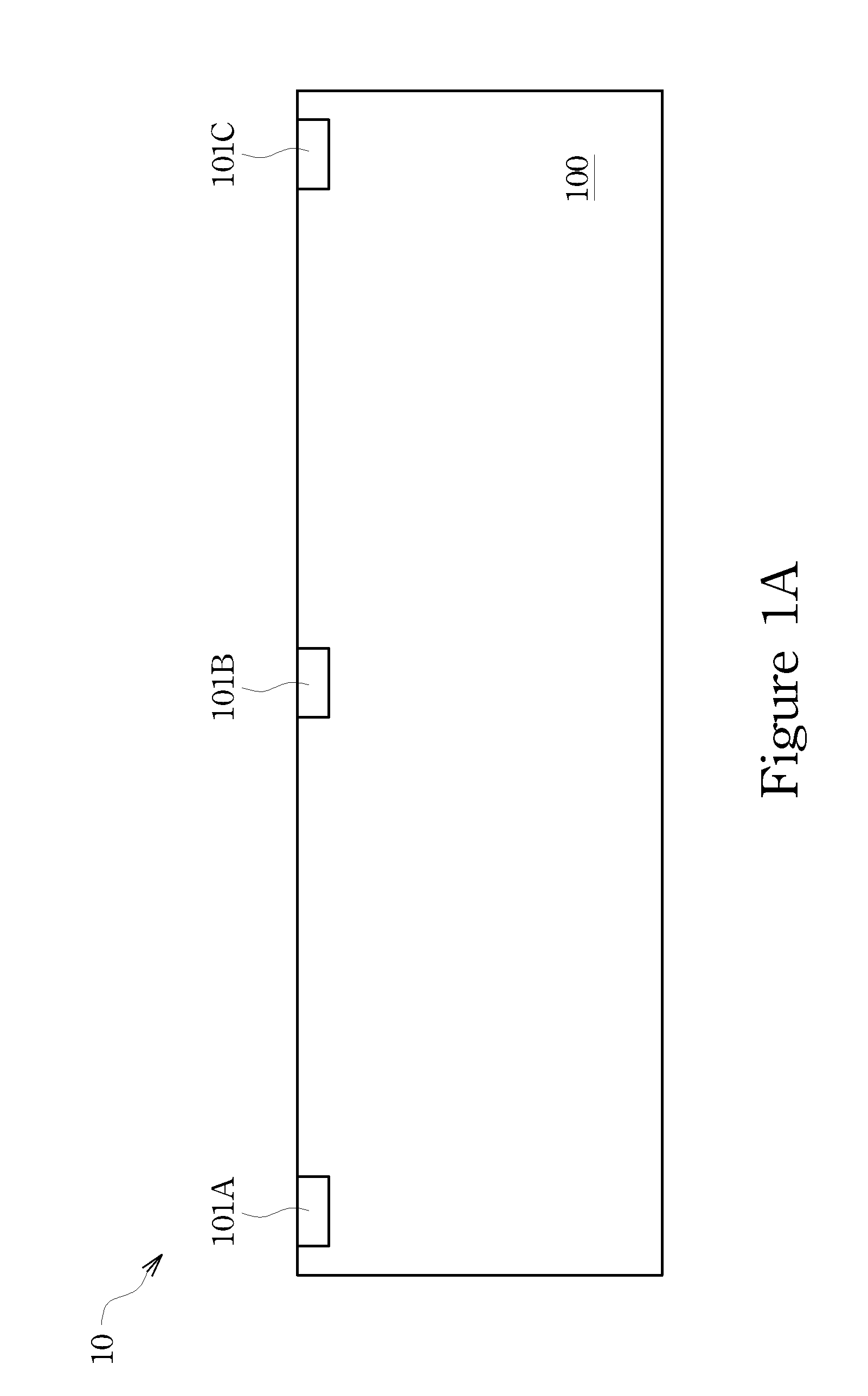
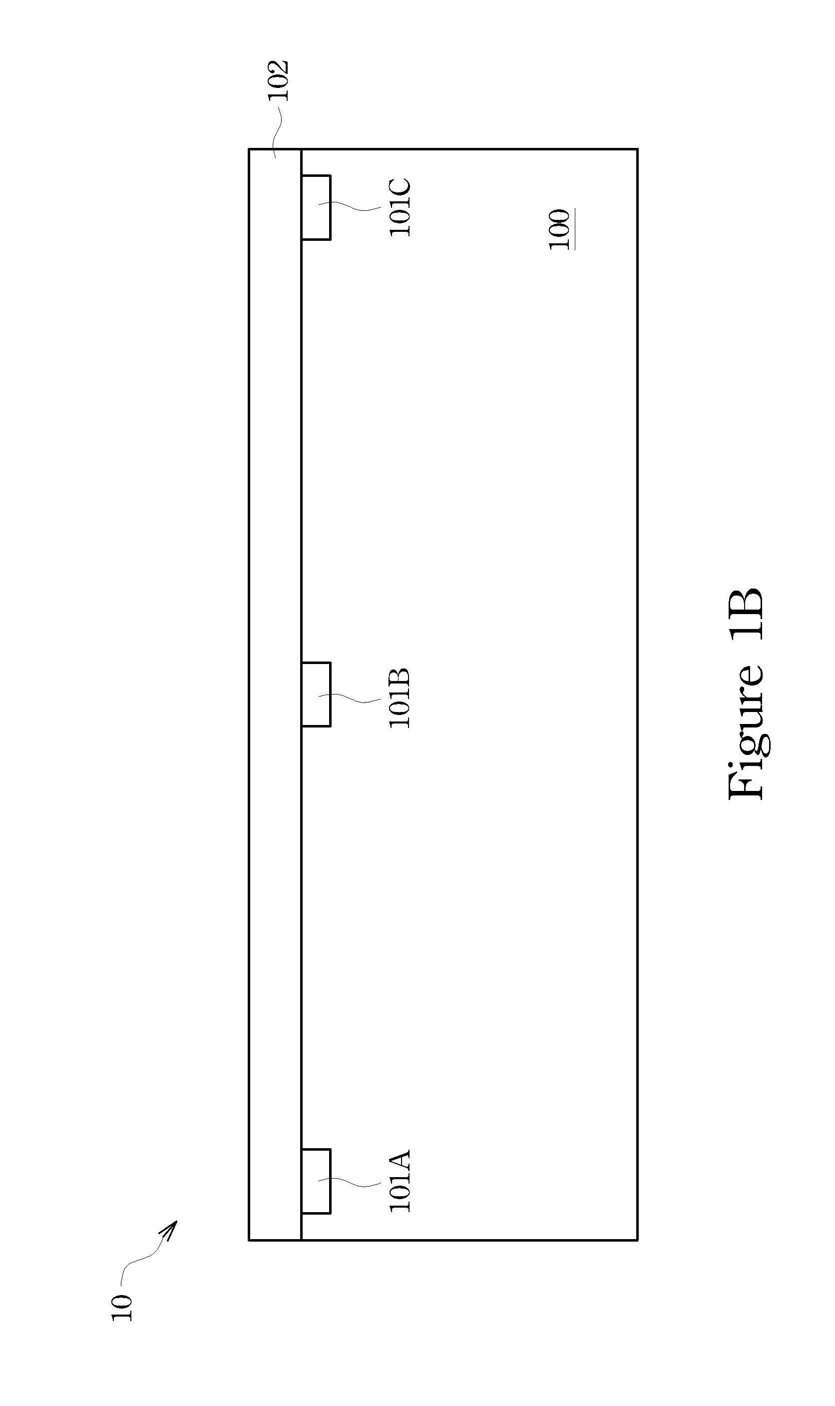
[0018]With reference now to FIG. 1A, there is shown a cross-sectional diagram of wafer 10. Wafer 10 comprises substrate 100, which is typically silicon (Si), but may also be made of gallium arsenide (GaAs), gallium arsenide-phosphide (GaAsP), indium phosphide (InP), gallium aluminum arsenic (GaAlAs), indium gallium phosphide (InGaP), and the like, and illustrates devices 101A, 101B, and 101C processed in substrate 100. In FIG. 1B, insulating layer (also sometimes referred to as inter-layer dielectric or ILD layer) 102 is deposited on substrate 100 of wafer 10. Examples of suc...


PUM


Abstract

The formation of through silicon vias (TSVs) in an integrated circuit (IC) die or wafer is described in which the TSV is formed in the integration process prior to metallization processing. TSVs may be fabricated with increased aspect ratio, extending deeper in a wafer substrate. The method generally reduces the risk of overly-thinning a wafer substrate in a wafer back-side grinding process typically used to expose and make electrical contacts to the TSVs. By providing deeper TSVs and bonding pads, individual wafers and dies may be bonded directly between the TSVs and bonding pads on an additional wafer.

Description

TECHNICAL FIELD[0001]The present invention relates generally to integrated circuit fabrication, and more particularly to a method of forming stacked dies having one or more through-silicon vias.BACKGROUND[0002]Generally, the speed at which an integrated circuit operates is influenced by the distance between the farthest separated components that communicate with each other on the chip. Laying out circuits as three-dimensional structures has been shown to significantly reduce the communication path length between on-chip components, provided the vertical distances between the layers are much smaller than the chip width of the individual layers. Thus, by stacking circuit layers vertically, the overall chip speed is typically increased. One method that has been used to implement such stacking is through wafer bonding.[0003]Wafer bonding is the joining together of two or more semiconductor wafers on which integrated circuitry has been formed. Wafers are typically joined by direct bondin...

Claims


Application Information

Patent Timeline
Patent Type & Authority Patents(United States)
IPC IPC(8): H01L21/02
CPCH01L21/76898H01L25/0657H01L25/50H01L2225/06513H01L2225/06517H01L2225/06541H01L2224/16225H01L2224/16145H01L2224/94H01L24/03H01L24/05H01L24/11H01L24/13H01L24/14H01L24/16H01L21/6835H01L24/81H01L24/92H01L24/94H01L2224/034H01L2224/0361H01L2224/05624H01L2224/05639H01L2224/05644H01L2224/05647H01L2224/05684H01L2224/13009H01L2224/13025H01L2224/131H01L2224/13109H01L2224/13116H01L2224/13144H01L2224/13147H01L2224/13184H01L2224/1403H01L2224/14181H01L2224/16146H01L2224/81801H01L2224/9202H01L2224/9222H01L2224/03616H01L2224/92222H01L2221/68327H01L2221/6834H01L2224/0401H01L2224/05572H01L2924/14H01L2224/81H01L2224/80H01L2924/00014H01L2924/0105H01L2924/01079H01L2924/014H01L2224/03H01L2224/11H01L2924/00012H01L2924/00
Inventor CHEN, MING-FACHEN, CHEN-SHIENCHIU, WEN-CHIH
Owner TAIWAN SEMICON MFG CO LTD
Why Eureka
Try Eureka