Method for fabricating a long-range ordered periodic array of nano-features, and articles comprising same

a nano-feature and feature technology, applied in the field of nanotechnology, can solve the problems of non-ordered patterning, interference and noise in the array of sub-50 nm nano-features fabricated according to conventional methods, and difficult to fabricate arrays of nano-features with less than 50 nm feature size with known lithography techniques,

Active Publication Date: 2012-05-15
RGT UNIV OF CALIFORNIA
View PDF15 Cites 10 Cited by
  • Summary
  • Abstract
  • Description
  • Claims
  • Application Information

AI Technical Summary

Problems solved by technology

However, arrays of nano-features with a less than 50 nm feature size are difficult to fabricate with known lithography techniques.
Specifically, arrays having sub 50 nm nano-features fabricated according to conventional methods generally include interference and noise caused by the interaction between adjacent nano-features.
However, processes such as those involving surfactant-mediated periodic ordering based on the evaporation of carrier solvent (e.g., hexane or octane) in a colloidal mixture including nano-particles (e.g., Co or Fe2O3 nano-particles) and a surfactant (e.g., fatty acids such as oleic acid, oleylamine, hexanoic acid, hexylamine) often suffer from the problem of multiple nucleation and growth of ordering reactions, which leads to non-ordered patterning.
However, a major drawback to the above-identified techniques is that the periodic arrays of nano-islands or nano-rods that may be formed are often very small in area, e.g., several micrometers.
The non-periodic arrangement of such memory devices, logic devices, and / or information bits increases the total number of device defects and reduces the effectiveness and usefulness of the nano-patterned device array.
For example, a non-periodic arrangement may cause undesirable electrical shorts, capacitive interactions, noises, and / or interference with neighboring elements.
In the case of magnetic hard disc media, undesirable switching or read error of magnetically written bits (magnetized along a desired direction) may occur if the neighboring magnetic islands are spaced too close together when the moving read / write head passes by the magnetic bits to retrieve the written information.
If the elements in the X-Y matrix array of devices are arranged in a non-periodic configuration, the device elements may be mis-registered with respect to the X-Y conductor array lines, causing the device to function in a undesirable manner.

Method used


Image

  • Method for fabricating a long-range ordered periodic array of nano-features, and articles comprising same
  • Method for fabricating a long-range ordered periodic array of nano-features, and articles comprising same
  • Method for fabricating a long-range ordered periodic array of nano-features, and articles comprising same

Examples


Embodiment Construction

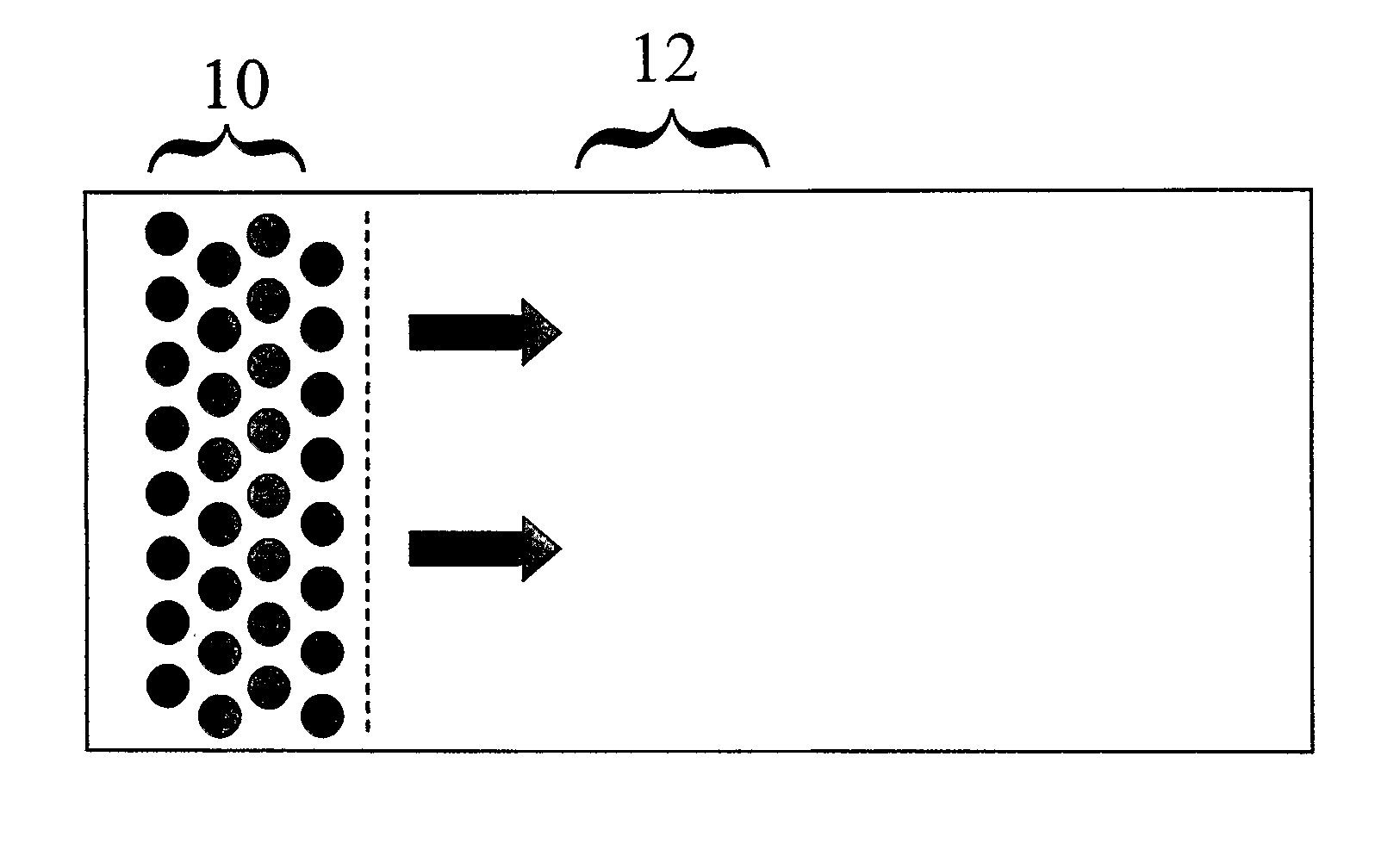
[0042]The present invention relates to methods for the fabrication of long-range, period array of discrete nano-features, such as, for example, nano-islands, nano-particles, nano-pores, nano-compositional modifications, and nano-device components. The term “nano-feature,” as used herein is intended to include any feature, structure, island, particle, pore, device component, composite, or other element that has a diameter or width of less than or equal to 100 nm, preferably less than or equal to 50 nm, and even more preferably less than or equal to 20 nm.

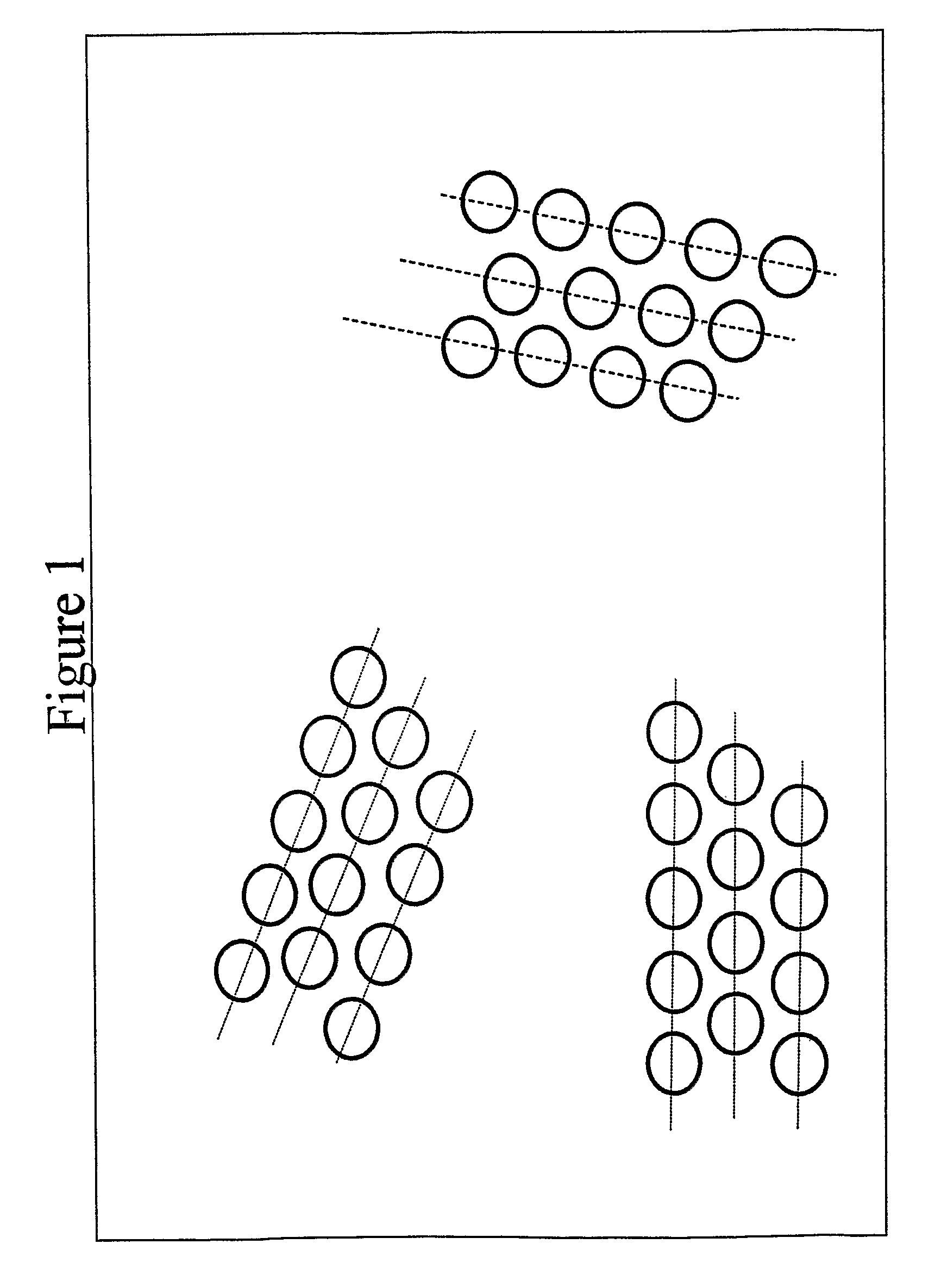
[0043]The terms “long-range ordered periodic array,”“long-range periodically ordered array,” and “long-range periodic array” as used herein are intended to include an ordered periodic array of nano-features having an area of at least approximately 1 mm2, preferably at least approximately 1 cm2, and even more preferably an area of at least approximately 4 cm2. The percentage of non-periodic defects (i.e., nano-features that are missin...


PUM

PropertyMeasurementUnit
diameteraaaaaaaaaa
feature sizeaaaaaaaaaa
hole diameteraaaaaaaaaa

Abstract

A long range, periodically ordered array of discrete nano-features (10), such as nano-islands, nano-particles, nano-wires, non-tubes, nano-pores, nano-composition-variations, and nano-device-components, are fabricated by propagation of a self-assembling array or nucleation and growth of periodically aligned nano-features. The propagation may be induced by a laterally or circularly moving heat source, a stationary heat source arranged at an edge of the material to be patterned (12), or a series of sequentially activated heaters or electrodes. Advantageously, the long-range periodic array of nano-features (10) may be utilized as a nano-mask or nano-implant master pattern for nano-fabrication of other nano-structures. In addition, the inventive long-range, periodically ordered arrays of nano-features are useful in a variety of nanoscale applications such as addressable memories or logic devices, ultra-high-density magnetic recording media, magnetic sensors, photonic devices, quantum computing devices, quantum luminescent devices, and efficient catalytic devices.

Description

CROSS-REFERENCE TO RELATED APPLICATIONS[0001]This application is a U.S. National Stage Application of PCT International Application No. PCT / US2006 / 002122, filed on Jan. 23, 2006, which in turn claims the benefit of U.S. Provisional Application Ser. No. 60 / 645,770, filed Jan. 21, 2005. U.S. patent application Ser. No. 60 / 645,770 and PCT Application No. PCT / US2006 / 002122 are incorporated by reference herein.FIELD OF THE INVENTION[0002]This invention relates to nanotechnology, particularly the formation of a periodic array of nano-features.BACKGROUND OF THE INVENTION[0003]Periodic arrays of nano-features, such as a nano-islands, nano-rods, and nano-cavities, are useful as a basis of a variety of nano-devices, including electronic, acoustic, photonic, and magnetic devices. Examples of such devices include quantum dot or single electron transistor array, photonic bandgap structures, non-linear acoustic devices, and ultra-high-density information storage media (e.g., magnetic recording me...

Claims


Application Information

Patent Timeline
Patent Type & Authority Patents(United States)
IPC IPC(8): B05D5/00B05D3/00
CPCB01J35/0013B01J37/0009B82Y10/00B82Y25/00B82Y30/00G11B5/855H01F1/009G06N99/002B01J23/40Y10S977/858H01F1/405Y10S977/849Y10S977/855G06N10/00
Inventor JIN, SUNGHO
Owner RGT UNIV OF CALIFORNIA
Why Eureka
Try Eureka