Method of fabricating conductive electrodes on the front and backside of a thin film structure

a thin film structure and fabrication method technology, applied in the direction of printed circuit details, printed circuit aspects, printed circuit manufacturing, etc., can solve the problems of metalized structures cracking, metalized structures failing to produce open circuit devices,

Active Publication Date: 2012-05-22
LAWRENCE LIVERMORE NAT SECURITY LLC
View PDF3 Cites 5 Cited by
  • Summary
  • Abstract
  • Description
  • Claims
  • Application Information

AI Technical Summary

Benefits of technology

[0010]The method of the present invention invention can be used to fabricate such thin film structures as high density, flexible and durable electrode arrays for use in applications such as for example high density neural stimulation and sensing using microelectrode neural probes to provide a direct electrical interface with the neurons of a biological entity's nervous system. In particular, whereas current neural electrode arrays produced using conventional MEMS techniques have exposed metal pads (e.g. signal recording or stimulation sites) located on a top side of rigid silicon shanks, neural electrode arrays fabricated according to the present invention have electrodes on both front and back surfaces, which can stimulate or record a larger population of neurons. Furthermore, a wide variety of sensors and electronics similar to but not limited to chemical or biological sensors can also be fabricated using a similar arrangement of front and back side sensing elements.

Problems solved by technology

However, conventional MEMS techniques used to fabricate the polymer, semiconductor, metal and / or dielectric material-based thin film structures of such devices typically produce electrical connections / electrodes only on a top surface (i.e. a front side / face) of the device.
However, this method has been known to lead to failure in the metalized structures to produce an open circuited device.
The physical stress involved in folding the substrate of the device can cause the metalized structures to crack and fail.

Method used


Image

  • Method of fabricating conductive electrodes on the front and backside of a thin film structure
  • Method of fabricating conductive electrodes on the front and backside of a thin film structure
  • Method of fabricating conductive electrodes on the front and backside of a thin film structure

Examples


Embodiment Construction

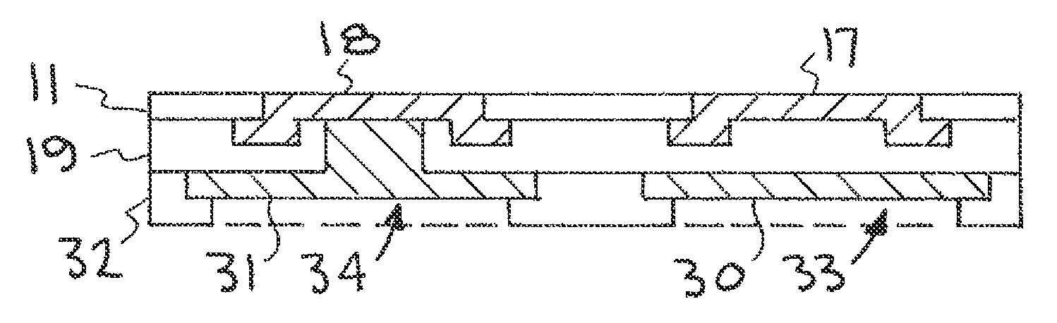
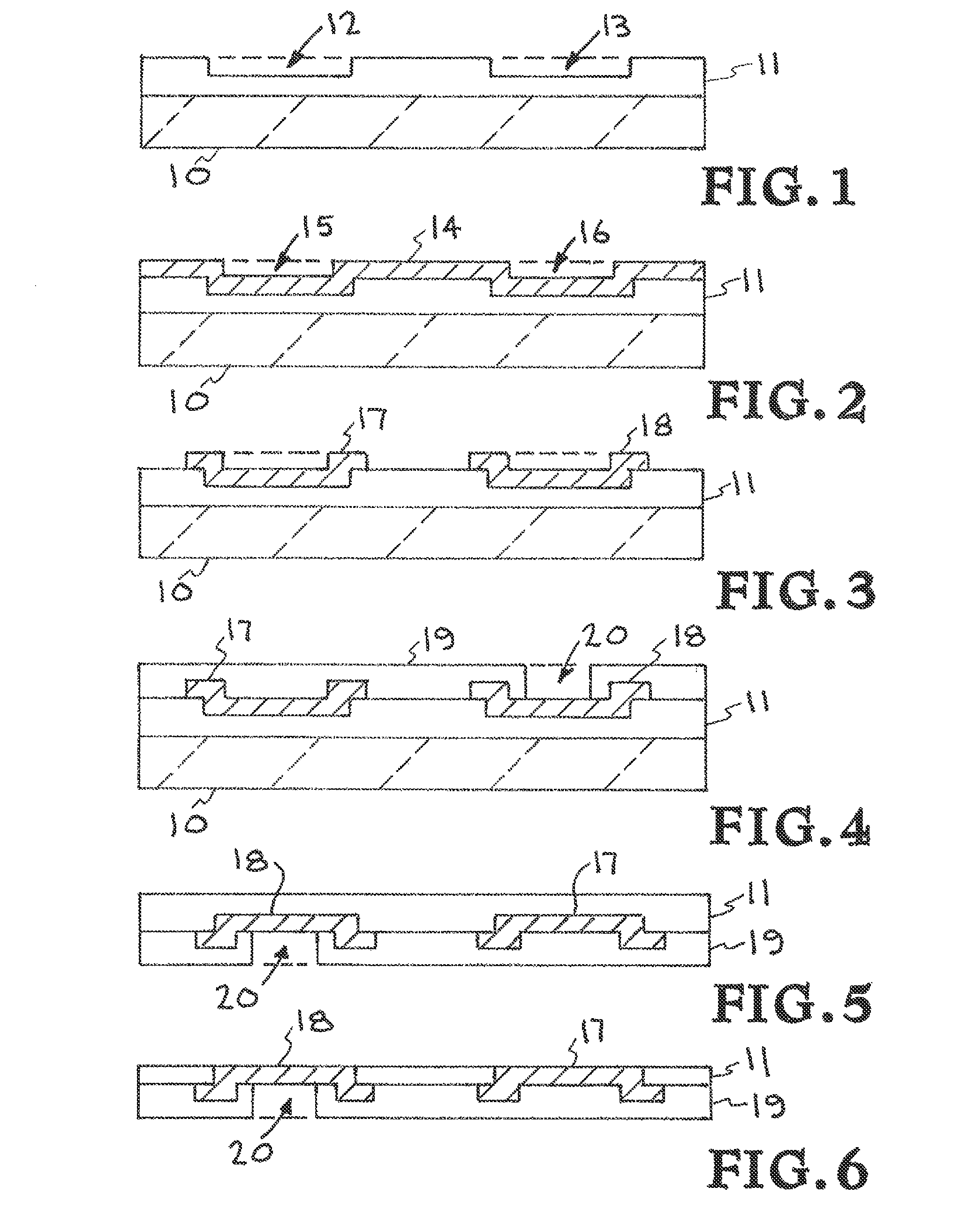
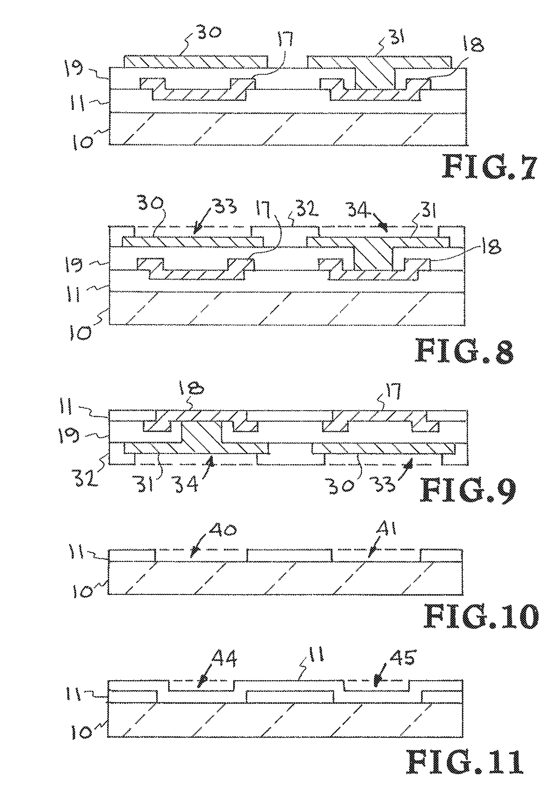
[0018]Turning now to the drawings, FIGS. 1-6 together show a first example embodiment of a method of fabricating a thin film structure having conductive electrodes on the front and backsides. In particular, six progressive stages are shown for producing an example single-level thin film structure, i.e. a thin film structure having a single layer of defined metal structures embedded between dielectric layers. It is appreciated however that additional layers of defined metal structures may be formed to produce a multi-level thin film structure and device, described in detail below.

[0019]FIG. 1 shows a first thin-film dielectric layer 11 deposited on a substrate 10 which may be a silicon, metal, glass or ceramic substrate. For this and subsequent dielectric layers, it is appreciated that any desired dielectric layer material may be used, such as but not limited to parylene, polyimide, polyethylene, polyurethane, silicon, silicon dioxide, silicon nitride, silicon carbide, quartz, boro-s...


PUM

PropertyMeasurementUnit
thicknessaaaaaaaaaa
angleaaaaaaaaaa
pressureaaaaaaaaaa

Abstract

A method of fabricating a thin film device having conductive front and backside electrodes or contacts. Top-side cavities are first formed on a first dielectric layer, followed by the deposition of a metal layer on the first dielectric layer to fill the cavities. Defined metal structures are etched from the metal layer to include the cavity-filled metal, followed by depositing a second dielectric layer over the metal structures. Additional levels of defined metal structures may be formed in a similar manner with vias connecting metal structures between levels. After a final dielectric layer is deposited, a top surface of a metal structure of an uppermost metal layer is exposed through the final dielectric layer to form a front-side electrode, and a bottom surface of a cavity-filled portion of a metal structure of a lowermost metal layer is also exposed through the first dielectric layer to form a back-side electrode.

Description

I. CLAIM OF PRIORITY IN PROVISIONAL APPLICATION[0001]This application claims priority in provisional application filed on Dec. 2, 2009, entitled “Different Methods of Fabricating Conductive Electrodes on the Front and Backside of Polymer, Semiconductor, Metal and Dielectric Based Devices” Ser. No. 61 / 266,003, by Phillipe J. Tabada et al, and in provisional application filed on Dec. 11, 2009, entitled “Fabrication of a Hybrid Silicone-Parylene Neural Prosthetic Device” Ser. No. 61 / 285,874, by Phillipe J. Tabada et al, both of which are incorporated by reference herein.II. FEDERALLY SPONSORED RESEARCH OR DEVELOPMENT[0002]The United States Government has rights in this invention pursuant to Contract No. DE-AC52-07NA27344 between the United States Department of Energy and Lawrence Livermore National Security, LLC for the operation of Lawrence Livermore National Laboratory.III. FIELD OF THE INVENTION[0003]The present invention relates to thin film structures and fabrication methods, and ...

Claims


Application Information

Patent Timeline
Patent Type & Authority Patents(United States)
IPC IPC(8): H01L21/336
CPCA61N1/0529H01L21/76814H05K1/11H05K3/4038H05K2201/0394
Inventor TABADA, PHILLIPE J.TABADA, LEGAL REPRESENTATIVE, MELODYPANNU, SATINDERPALL S.
Owner LAWRENCE LIVERMORE NAT SECURITY LLC
Why Eureka
Try Eureka